Figures & data
Figure 1 Electrode and electrolyte interface showing faradaic charge injection and capacitive charge injection (a), and a two-element electrical circuit model of electrode/electrolyte interface (b). Note: Reprinted by permission of Merrill et al. (Citation2005).
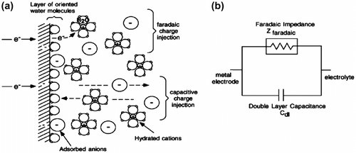
Figure 2 Impedance spectra of smooth platinum, Pt black, IrOx and PPy/PSS-coated electrodes in phosphate buffered saline (conductivity: 1.6 S/m), impedance magnitude (a), and impedance phase (b). Note: Reprinted by permission of Malleo et al. (Citation2010).
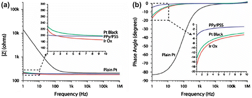
Table 1. Effective interfacial capacitance for each material in 1 M NaCl and 1x PBS (Malleo et al., Citation2010).
Figure 3 Examples of 3D out-of-plane and in-plane electrode arrays. Note: (a) The Utah Electrode Array (UEA) for high-density neural recording and stimulation is a silicon-based device of 3D out-of-plane type. It has a 10 × 10 array of tapered silicon electrodes with a base width of 80 μm, a height of 1500 μm and an electrode pitch of 400 μm. Reprinted by permission of Badi et al. (2003). (b) Schematic view of a multielectrode stimulating neuroprobe and a scanning electron microscope (SEM) image of the tip of a multisite probe with a thickness of 15 μm and a distance of 200 μm between the electrode sites. Reprinted by permission of Tanghe, Najafi, and Wise (Citation1990)
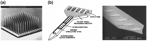
Figure 4 3D neural probe consisting of a thick shank (48 × 68 μm) and a thin lateral platform with subcellular dimensions (5× 100 μm). Note: Scale bar = 100 μm. Reprinted by permission of Seymour and Kipke (Citation2007).
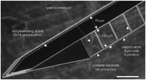
Figure 5 Highly porous surface of sputtered TiN resulting in a large effective electrode surface area. Note: (a) SEM image of TiN surface. Reprinted by permission of Schaldach, Hubmann, Weikl, and Hardt (Citation1990). (b) Schematic of a pore cross-section with pore resistance R and double-layer capacitance C. Modified from Cogan (Citation2008).
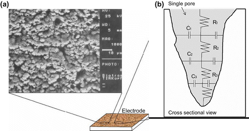
Figure 6 Classification of available fabrication technologies for neuroprosthetics based on the length scale of machinable structures. Modified from Stieglitz (Citation2010).
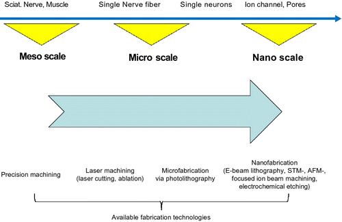
Figure 7 Flexible electrode arrays.
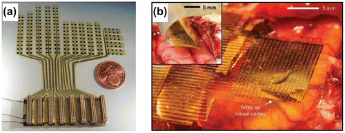
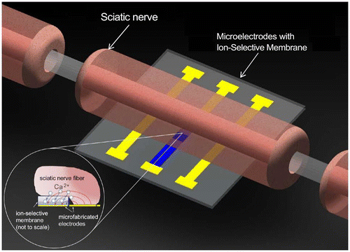
Figure 8 Electrochemical stimulation of sciatic nerve using ion-selective membrane.