Figures & data
Figure 1. Schematic of the experimental device.
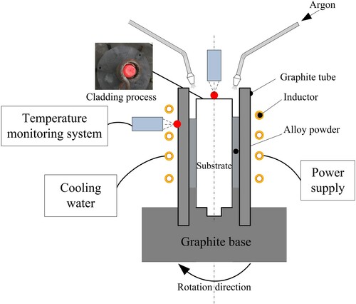
Table 1. Nominal chemical composition of Co 158 and AISI 1045 steel (wt.%).
Table 2. Experimental parameters.
Figure 2. Schematic of sample-cutting approach.
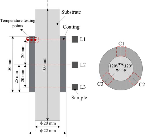
Figure 3. Material parameters of the (a) substrate and (b) coating.
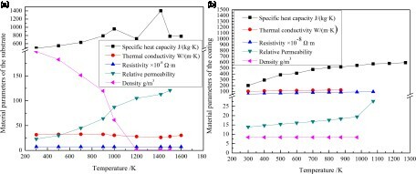
Figure 4. 2D geometric model and boundary.
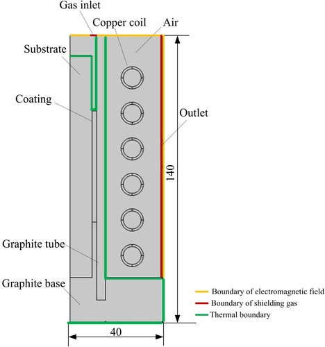
Figure 5. Entire model with an unstructured grid and the enlarged views.
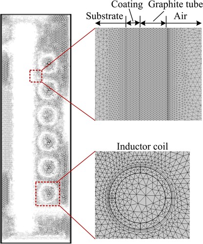
Figure 6. Element quality histogram.
Figure 7. Electromagnetic, temperature, and gas flow fields at t = 210 s: J is the current density, Φ is the magnetic flux, T is the temperature, and v is the velocity of the sheilding gas.
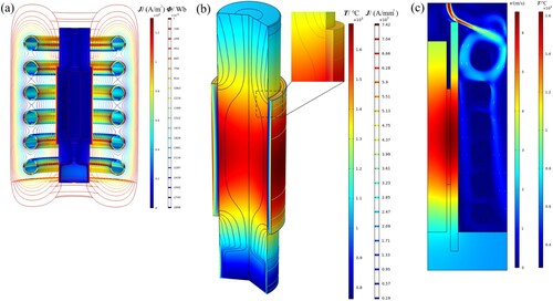
Figure 8. Current density evolution in the cross section of the coating at L2.
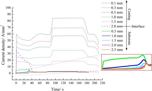
Figure 9. Skin depth δ profile.
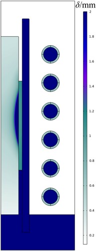
Figure 10. Maximum temperature of the coating at various positions.
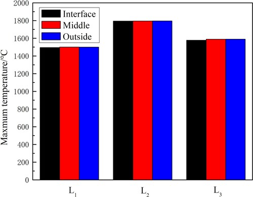
Figure 11. Experimental and simulated time–temperature curves.
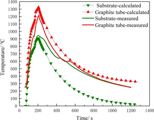
Figure 12. Line scanning results at the interface in: (a) L1, (b) L2, and (c) L3.
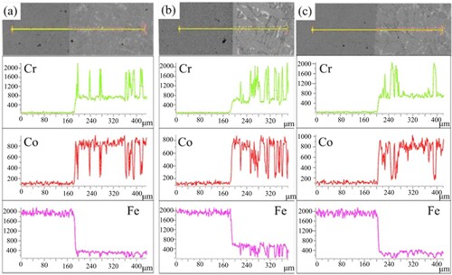
Figure 13. XRD patterns of coating surface in: (a) L1, (b) L2, and (c) L3.
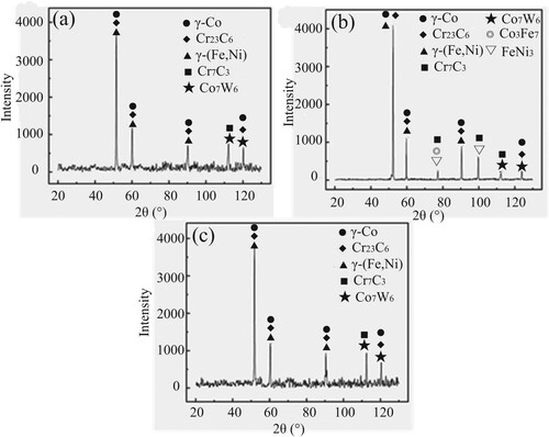
Figure 14. SEM image of a selected area in the coating at L2 and the corresponding EDS analysis results.
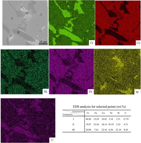
Figure 15. Porosity of the Co-based coating at various locations.
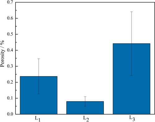
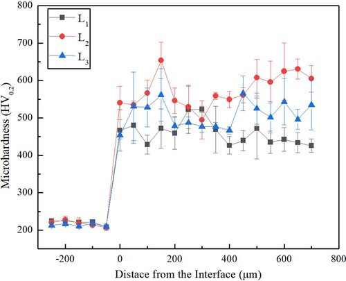
Figure 16. Microhardness profile of Co-based sample.