Figures & data
Figure 1. LSP process [Citation14].
![Figure 1. LSP process [Citation14].](/cms/asset/a35f682a-dab7-4136-9ed1-1d3eb7cf74d9/ysue_a_2060463_f0001_oc.jpg)
Figure 2. Schematic of (a) cross-section of the sample and photograph of (b) produced sample with a fabricated notch.
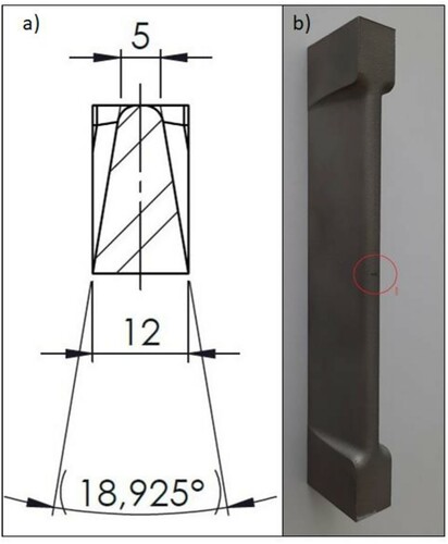
Table 1. Process parameters used for the manufacturing of AM samples.
Figure 3. Schematic representation of the experimental set-up.
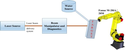
Figure 4. Photograph of (a) creation of LSP patch and (b) samples prepared for fatigue testing.
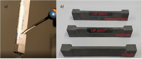
Table 2. LSP parameters used for the processing.
Figure 5. Schematic of (a) 4-point bending test loading scheme and photograph of (b) 4-point bend test rig RUMUL.
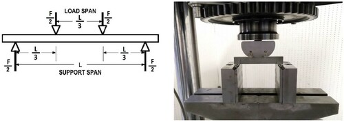
Figure 6. Residual stress distribution for AB, AlT, and VT.
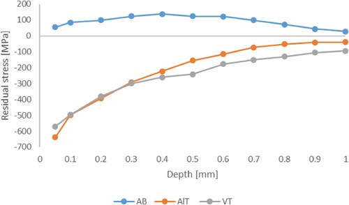
Figure 7. Graphical representation of the fatigue test results.
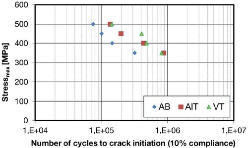
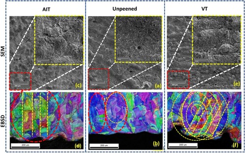
Figure 8. (a,c,e) The SEM micrographs of unpeened, LSP treated with AIT, and LSP treated with VT, respectively. (b,d,f) EBSD micrographs of the same three samples.