
Figures & data
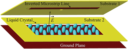
Table 1. Power consumption of active arrays using different phase shift technologies.
Table 2. The common measurement techniques to characterise LCs.
Figure 1. The chemical structure of the LC monomer, QYPD-036.
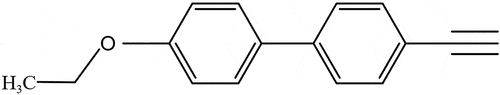
Table 3. The comparison of the recently available NLCs and the classical display mixtures E7 (Merck) for display and photonic applications.
Figure 2. (Colour online) Design 1 of an NLC-based IMSL: on Substrate 1, the inverted microstrip line and the CPW for measurement are on two sides of the board, and they are connected through a via. Substrate 2 is to provide a cavity in the middle board to contain the NLC mixture, and the bottom board is working as a metallic ground plane.
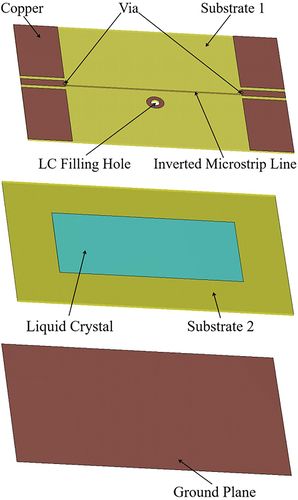
Figure 3. (Colour online) The inverted microwstrip line, NLC in the cavity and the electric fields of the waves propagating through.
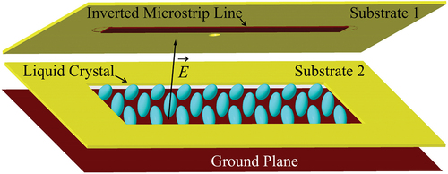
Figure 4. (Colour online) The detailed dimensions of the IMSL designs: case 1 refers to the vias used in Design 1, and case 2 refers to the coupling mechanism employed in Design 2.
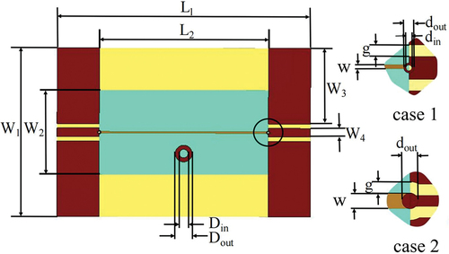
Table 4. The dimensions of the two IMSL designs in millimetres.
Figure 5. Cross section of the inverted microstrip line structure under two scenarios: (a) the empty cavity and (b) the cavity was filled with LCs.
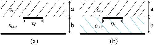
Table 5. The factor to calculate the effective length of IMSLs under the two scenarios.
Figure 6. (Colour online) Fabrication process of the IMSL device based on Design 1: (a) top view of Substrate 1, (b) bottom view of Substrate 1, (c) the top surface of the board of ground plane was spin-coated with a thin layer of PI and (d) the bias voltage being applied on an IMSL device based on Design 1.
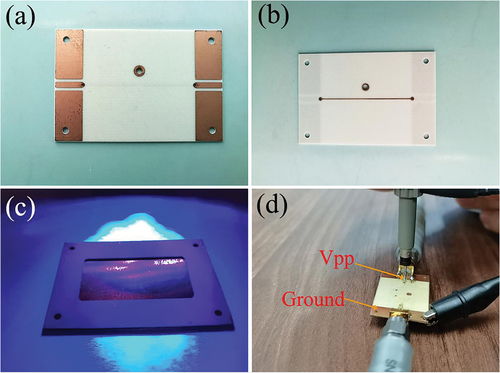
Figure 7. (Colour online) Fabrication process of the IMSL devices based on Design 2: (a) top view of Substrate 1, (b) bottom view of Substrate 1, (c) the top surface of the board of ground plane was spin-coated with a thin layer of PI and (d) a completed IMSL device based on Design 2.
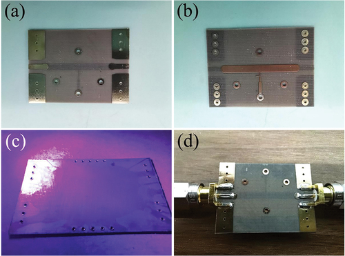
Table 6. The dielectric properties of the JC-M-LC-E7 LC determined based on the measurements of the IMSL devices.
Table 7. The dielectric properties of the QYPD-036 LC determined based on the measurements of the IMSL devices.
Figure 8. (Colour online) The comparison of scattering parameter of the empty IMSL device (Design 1, air in the cavity) between simulation and measurement.
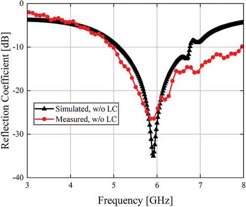
Figure 9. (Colour online) Simulated and measured scattering parameters of the IMSL device (Design 1) with JC-M-LC-E7 being filled in the cavity, under 0 and 20 V () bias voltage applied, respectively.
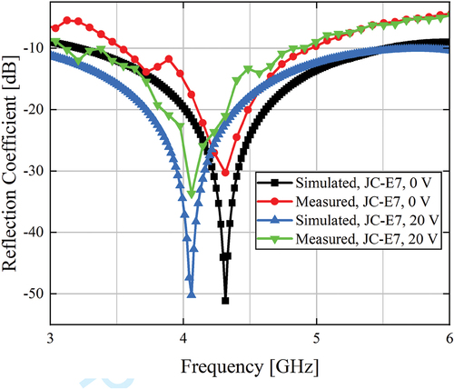
Figure 10. (Colour online) The comparison of scattering parameter of the empty IMSL device (Design 2, air in the cavity) between simulation and measurement.
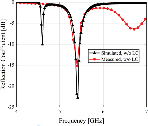
Figure 11. (Colour online) Simulated and measured scattering parameters of IMSL device (Design 2) with JC-M-LC-E7 LC being filled in the cavity, under 0 and 32 V () bias voltage applied, respectively.
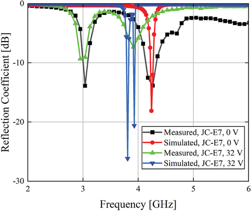
Figure 12. (Colour online) Fabricated NLC-based IMSL devices: (a) the three devices based on Design 1 and (b) the two devices based on Design 2.
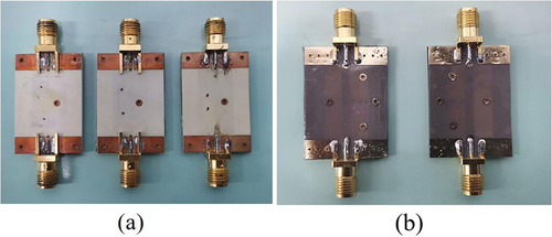
Figure 13. (Colour online) The difference between the measured and simulated results of resonant frequency for the empty DUTs (the Design 1 of IMSL, air in the cavity).
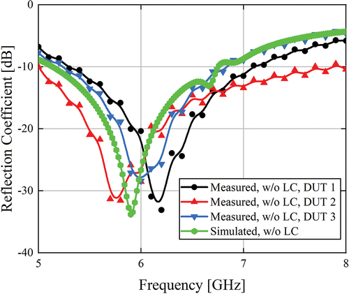
Figure 14. (Colour online) The difference between the measured and simulated results of resonant frequency for the empty DUTs (the Design 2 of IMSL, air in the cavity).
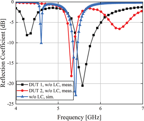
Table 8. The uncertainty analysis based on the IMSL devices of Design 1.
Table 9. The uncertainty analysis based on the IMSL devices of Design 2.