Figures & data
FIG. 1 Particle distribution in volume percent (% v/v); (a) wide distribution of larger SAC particles with a mean diameter of 15.6 μm; (b) narrow distribution of small SAC particles with a mean diameter of 2.3 μm.
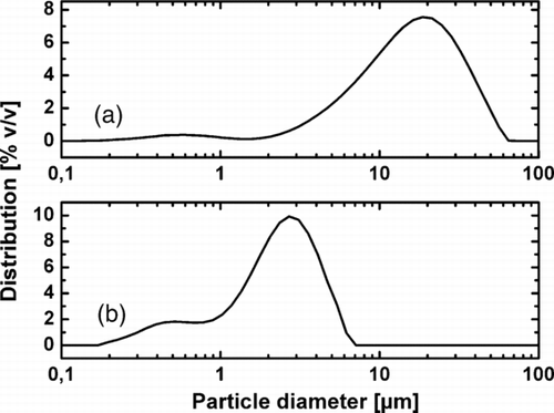
FIG. 2 (top) CMOS chip with SAC particle deposition pattern with a total of 16,384 pixels on 1.28 × 1.28 cm2; (bottom) schematic deposition; two different kinds of particles are deposited on defined pixels consecutively.
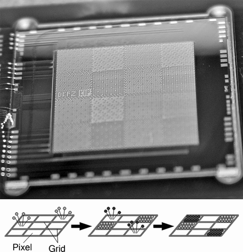
FIG. 3 Principle of aerosol generation; particles are sucked out of a reservoir through an ejector, the aerosol is guided through a Teflon tube to the outlet, where the aerosol is brought into contact with the chip surface.
FIG. 4 Schematic geometry of aerosol outlet and CMOS chip position above the air stream for particle deposition.
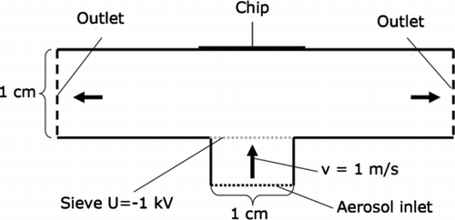
FIG. 5 Simulation for the specific geometry as shown in ; (a) air velocity field; (b) electrostatic potential.
FIG. 6 Desired particle deposition pattern (a, left) and experimentally achieved pattern (a, right); (b) schematic of particle deposition on a chip; particles move towards the chip and are manipulated by electrical fields resulting from the voltage pattern on the chip surface to enable spatial defined particle deposition.
FIG. 7 Simulation detail of particle deposition on a chip; particles are 10 μm in diameter and feature a q/m value of –3.10–3 C/kg; (a) the voltage of the grid electrode is 0 V, several particles are deposited as contaminations on deactivated pixels; (b) voltage of the grid electrode is 30 V, excess particles are solely deposited on the grid electrode.
FIG. 8 Simulation of particle deposition on a chip; particle trajectories are represented as black lines, grayscale represents the electrical potential [V]; particle diameters are (a) 3 μm, (b) 5 μm, (c) 10 μm; with q/m value of –3.10–3 C/kg; in all cases no contamination on grounded pixels occurs.
![FIG. 8 Simulation of particle deposition on a chip; particle trajectories are represented as black lines, grayscale represents the electrical potential [V]; particle diameters are (a) 3 μm, (b) 5 μm, (c) 10 μm; with q/m value of –3.10–3 C/kg; in all cases no contamination on grounded pixels occurs.](/cms/asset/95b0ceac-915e-436f-9fc2-37f08715b624/uast_a_517814_o_f0008g.gif)
FIG. 9 Simulation of particle deposition on a chip; particle trajectories are represented as black lines, grayscale represents the electrical potential [V]; particle diameters are (a) 3 μm, (b) 5 μm, (c) 10 μm; with q/m value of –3.10–2 C/kg; in (a, b) no contamination on grounded pixels occurs in contrast to (c).
![FIG. 9 Simulation of particle deposition on a chip; particle trajectories are represented as black lines, grayscale represents the electrical potential [V]; particle diameters are (a) 3 μm, (b) 5 μm, (c) 10 μm; with q/m value of –3.10–2 C/kg; in (a, b) no contamination on grounded pixels occurs in contrast to (c).](/cms/asset/d4fb4844-de13-4544-a609-1a7509d03213/uast_a_517814_o_f0009g.gif)
TABLE 1 Stopping distance S for different particle diameters d with corresponding Knudsen number Kn and Cunningham correction factor Cc; initial velocity is v = 1m/s
FIG. 10 Simulation of particle deposition on a chip; the electrostatic potential [V] is shown in grayscale, particle trajectories are shown as black lines; particles are 10 μm in diameter and possess a q/m value of –3.10–3 C/kg; (a) the voltage of the sieve is –1 kV, several particle trajectories end on the chip surface; (b) the voltage of the sieve is 0 V, only one single particle trajectory ends on the chip surface; (c) schematic of a particle in the electrical field resulting from the charge of the aerosol and the chip surface, acting as opposing electrodes.
![FIG. 10 Simulation of particle deposition on a chip; the electrostatic potential [V] is shown in grayscale, particle trajectories are shown as black lines; particles are 10 μm in diameter and possess a q/m value of –3.10–3 C/kg; (a) the voltage of the sieve is –1 kV, several particle trajectories end on the chip surface; (b) the voltage of the sieve is 0 V, only one single particle trajectory ends on the chip surface; (c) schematic of a particle in the electrical field resulting from the charge of the aerosol and the chip surface, acting as opposing electrodes.](/cms/asset/055fd26f-54f9-4fed-99c3-103211d8e709/uast_a_517814_o_f0010g.gif)
FIG. 11 Simulation of particle deposition on a chip; the electrostatic potential [V] is shown in grey scale, particle trajectories are shown as black lines; particles are 5 μm in diameter and possess a q/m value of –3.10–3 C/kg; (a) one pixel with 100 V is neighbored by 0 V pixels; particles tend to be deposited on the middle of the 100 V pixel; (b) three adjacent pixels with 100 V are neighbored by 0 V pixels; particles are deposited equally distributed on the 100 V pixel in the center, particles deposited on the left and right 100 V pixel tend to be deposited on the side of the pixel, into direction of the center pixel.
![FIG. 11 Simulation of particle deposition on a chip; the electrostatic potential [V] is shown in grey scale, particle trajectories are shown as black lines; particles are 5 μm in diameter and possess a q/m value of –3.10–3 C/kg; (a) one pixel with 100 V is neighbored by 0 V pixels; particles tend to be deposited on the middle of the 100 V pixel; (b) three adjacent pixels with 100 V are neighbored by 0 V pixels; particles are deposited equally distributed on the 100 V pixel in the center, particles deposited on the left and right 100 V pixel tend to be deposited on the side of the pixel, into direction of the center pixel.](/cms/asset/61c04954-ef55-4a12-acc3-81f55771ffc8/uast_a_517814_o_f0011g.gif)
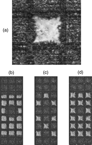
FIG. 12 Four different deposition patterns of micro particles on each chip surface (checkerboard, 1 of 16, 1 of 36, 1 of 64). (a) high degree of contamination; particles with a wide size distribution and a mean diameter of 15.6 μm were used; (b) almost free of contamination; particles with a narrow size distribution and a mean diameter of 2.3 μm were used.
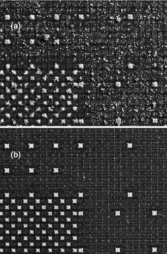
FIG. 13 Deposition on a chip (mean particle diameter 2.3 μm) exhibiting the effect described in the simulations in ; (a) single pixel with the pincushion effect visible; (b) in dependence of the voltage of directly surrounding pixels, particles either tend to be deposited in the center or on the side of the pixel; to guarantee isotropic central coverage of pixels, the same deposition pattern is produced by two consecutive deposition steps (c) and (d).