Figures & data
FIG. 1. Schematic of the experimental setup. An electrospray source operated inside a vacuum chamber produces a beam of charged nanodroplets, which upon acceleration strikes a target. The velocity of the droplets is measured with a time-of-flight spectrometer.
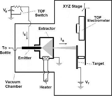
FIG. 2. (a) Time-of-flight waves of the EAN and EMI-Im beamlets, and of the ionic liquid TPP. The total acceleration voltage VA is just the emitter to extractor potential, VE. (b) Mass-to-charge ratio distributions for EAN and EMI-Im. The area under the distribution is the mass flow rate of the beamlet.
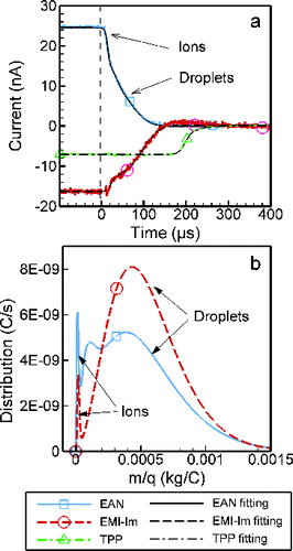
TABLE 1 Relevant physical properties of EAN and EMI-Im: molecular formula and mass, (amu); estimated molecular diameter,
(nm); density, ρ (kg/m3); surface tension, γ (N/m); electrical conductivity, K (S/m)
TABLE 2 Beamlet parameters: electrospray current, IE (nA); droplet current and mass flow rate, ID (nA) and (kg/s); average charge-to-mass ratio and typical droplet diameter,
(C/kg) and d (nm); number of molecules in the droplet,
; acceleration voltage,
(kV); average droplet velocity,
(km/s); molecular kinetic energy,
(eV); stagnation pressure
(GPa). The pairs of values in the last four columns correspond to the lowest and highest acceleration voltage
FIG. 3. Photographs and profilometer measurements of areas sputtered by the EMI-Im and EAN beamlets on a germanium target, at different acceleration potentials.
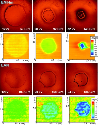
FIG. 4. Roughness of the Si, GaAs, Ge, and SiC surfaces bombarded by EAN and EMI-Im beamlets, as a function of the projectile's stagnation pressure.
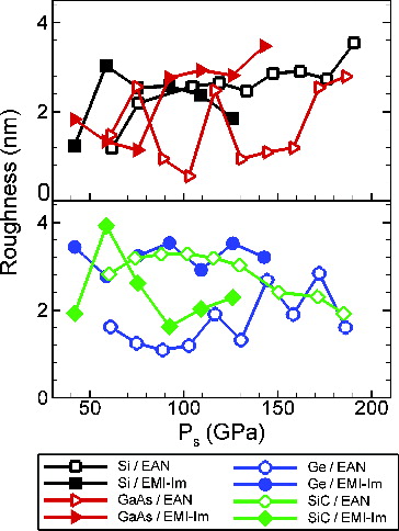
FIG. 5. Sputtering of Si, GaAs, Ge, and SiC by nanodroplets of EAN and EMI-Im, plotted in the form of (a) sputtering yield vs. molecular kinetic energy, and (b) total sputtering by a droplet 10 nm in diameter, as a function of its kinetic energy.
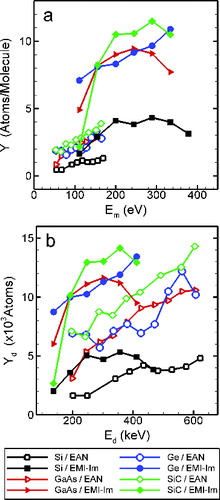
FIG. 6. Sputtering rates on Si, GaAs, Ge, and SiC, bombarded by beamlets of EAN and EMI-Im nanodroplets.
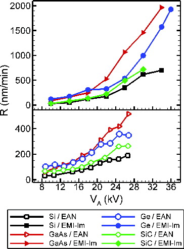
FIG. 7. Molecular dynamics simulations of the impact of EAN and EMI-Im nanodroplets on silicon. The projectiles are 10 nm in diameter and have an identical kinetic energy of 249 keV (11.0 km/s impact velocity for EAN and 10 km/s for EMI-Im). The snapshots are taken at 0.4, 1, 5, and 8 d/v time units. Panels a, c, e, and f correspond to EAN, while the impact of the EMI-Im drop is captured in panels b, d, f, and h.
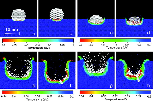
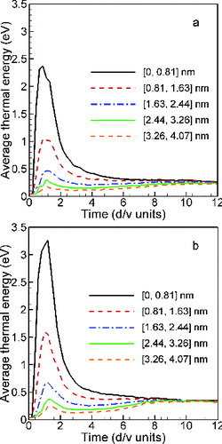
FIG. 8. Evolution of the average thermal energy per atom at varying depth from the surface. (a) Impact of the EAN projectile; (b) impact of the EMI-Im projectile.