Figures & data
FIG. 1. Schematic diagram for measuring the mean charge per particle.
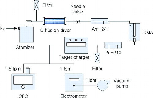
FIG. 2. SEM images of a silver nanowire (a) and dm = 200 nm, (b)
and dm = 300 nm, (c)
and dm = 200 nm, (d)
and dm = 300 nm, (e)
and dm = 200 nm, and (f)
and dm = 300 nm.
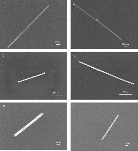
FIG. 3. Histograms for silver nanowires with silver nanowire length, (a) dm = 200 nm, (b) dm = 250 nm, (c) dm = 300 nm, and (d) silver nanowire diameter.
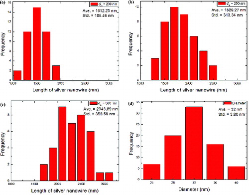
FIG. 4. Histograms for silver nanowires with silver nanowire length (a) dm = 200 nm, (b) dm = 300 nm, (c) dm = 400 nm, and (d) silver nanowire diameter.
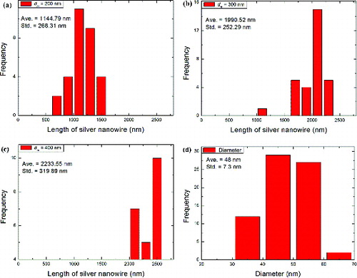
FIG. 5. Histograms for silver nanowires with silver nanowire length (a) dm = 200 nm, (b) dm = 300 nm, (c) dm = 400 nm, and (d) silver nanowire diameter.
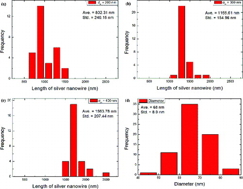
FIG. 6. Electrical capacitance of a spherical particle with a diameter of 40, 70, and 100 nm (symbol) and a nanowire with (line).
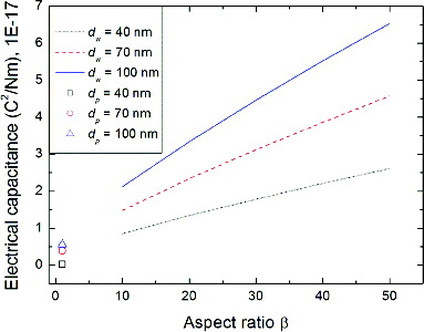
FIG. 7. The electrical capacitance of silver nanowires and PSL particles by theoretical analysis at an electrical mobility diameter (dm) of 200, 300, and 400 nm.
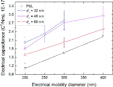
FIG. 8. The electrical capacitance of silver nanowires expressed as a function of the aspect ratio.
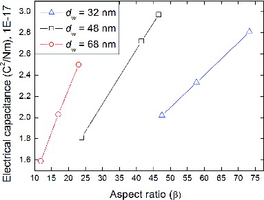
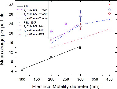
FIG. 9. Comparison of predicted results and experimental data for the mean charge per particle of silver nanowires and PSL particles using particle morphology information from SEM image analysis (line), and the experimental results for the mean charge on the silver nanowires and PSL particles (symbol).