
Figures & data
Figure 1. Basic three stage SST architecture.
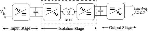
Figure 2. Schematic of isolated half-bridge converter and its associated waveforms.
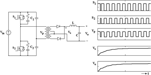
Figure 3. Plot of core geometry coefficient with frequency.
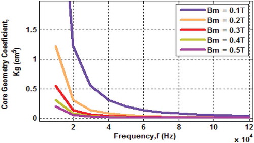
Figure 4. Flowchart for the proposed design optimization of high frequency transformer.
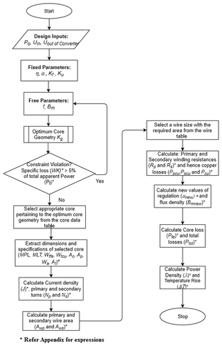
Table 1. Design specifications of a single converter module.
Table 2. Fixed parameters for optimization.
Table 3. Comparison of performance of optimization algorithms.
Table 4. Optimal core data.
Table 5. Optimal transformer characteristics.
Figure 5. Convergence plot of the optimization algorithms.
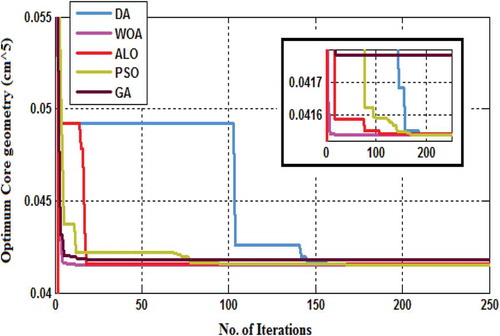
Figure 6. (a) Convergence plot in successive runs. (b) Time plot of convergence in successive runs.
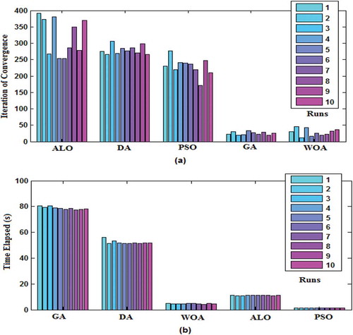
Figure 7. Schematic of the half-bridge DC–DC converter implemented in PowerEsim.
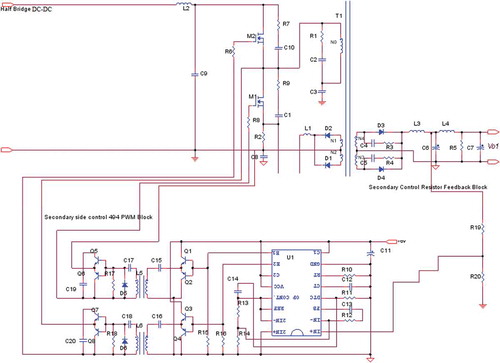
Figure 8. (a) Output switching ripple voltage waveform. (b) Input voltage (CH1) and input current (CH2) waveforms. (c) %Efficiency vs. input voltage. (d) Total dissipated losses vs. input voltage. (e) Output voltage regulation. (f) Variation of peak flux density of the transformer with respect to input voltage.
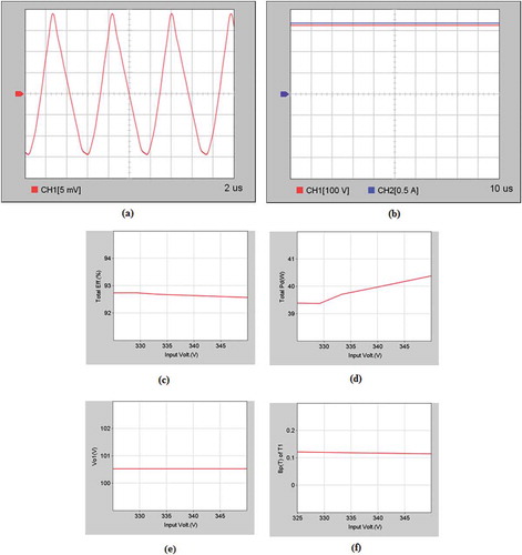
Figure 9. Winding arrangement of HF transformer.
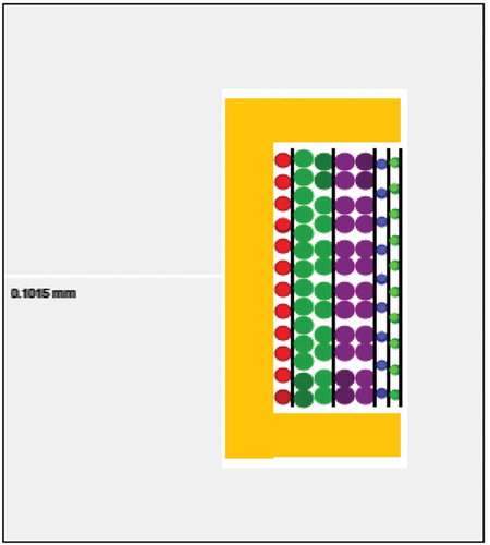
Figure 10. HF transformer design with PowerEsim.
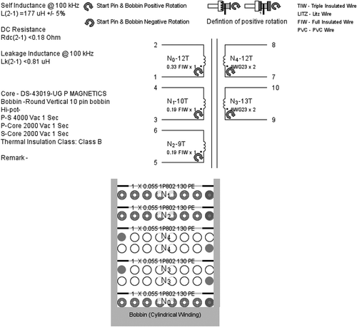
Table 6. Specifications of power circuit components.
Table 7. MTBF analysis of the overall circuit.
Table 8. MTBF analysis of the HF Transformer.