Figures & data
Figure 1. Schematic of the radiofrequency magnetron sputtering machine used in this study.
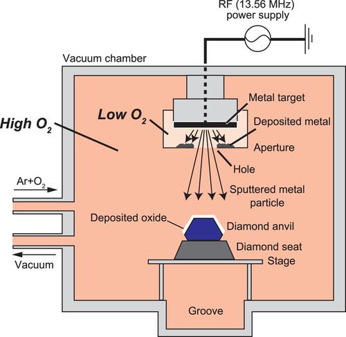
Figure 2. (a) Optical microscope image of the deposited alumina layer on the diamond anvil surface in run A8 with a scale of 100 μm. The bright spot on the left side of the culet is due to the oblique incident light from the optical microscope. (b,c) Secondary electron microscope image of cross-sections of (b) alumina and (c) zirconia layers on a single crystal diamond substrate milled by focused ion beam in run A9 and A10, respectively. Gold was deposited on top of the ZrO2 layer to prevent charge-up.
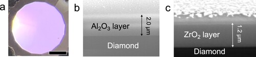
Table 1. Size of the radiofrequency magnetron sputtering machine.
Table 2. Conditions and results of alumina and zirconia sputtering.
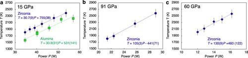
Figure 3. The laser power-temperature relations when sputtered (a) 2 μm-thick alumina and zirconia layers in run B1, and 2.3 μm-thick zirconia layer in run B2 at (b) 91 GPa, and (c) 60 GPa.