Figures & data
Figure 1. Schematic diagram of the proposed LC based tunable narrowband BSF.
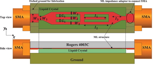
Figure 2. Prototype of (a) Spurline structures and (b) embedded spurline structures.
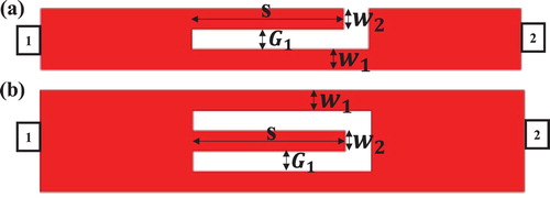
Figure 3. S-parameters comparison of the spurline and embedded spurline structure prototype.
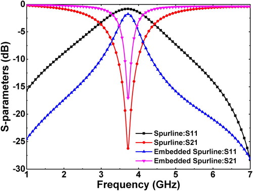
Figure 4. Current distribution at the rejection frequency of 3.725 GHz for (a) the spurline structure and (b) embedded spurline structure prototype.
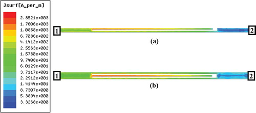
Figure 5. The effects of (a) gap , and (b) resonator width
, for the notch characteristics of the embedded spurline unit, and (c) current distributions at a stopband frequency of 3.725 GHz.
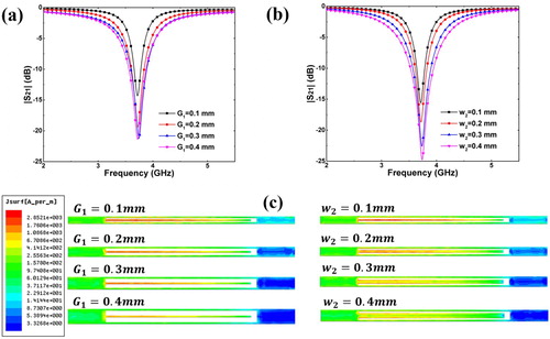
Figure 6. Comparison of structures with two embedded spurline units (a) in series and (b) In parallel, and (c) transmission, and (d) Current distributions.
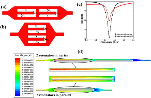
Figure 7. (a) The transmission characteristics of the embedded spurline unit, and (b) Current distributions at the rejection frequency, when varying the LC dielectric loss tangent .
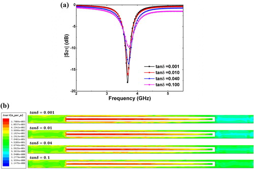
Figure 8. Experimental setup for measurement.
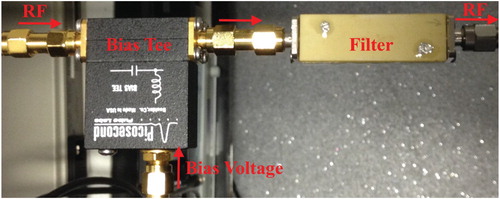
Figure 9. Measured results of the device with respect to the LC bias voltage: (a) Transmission, (b) stopband rejection frequency, and (c) stopband 3 dB bandwidth and Q factor.
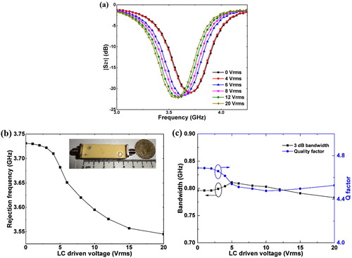
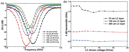
Figure 10. Measured results of devices with three LC layer thicknesses: (a) Transmission under 0 and 20 Vrms bias voltage, and (b) stopband 3 dB bandwidth with respect to various LC bias voltages.