
Figures & data
Figure 1. A schematic representation of the directions referred to in Voigt notation.
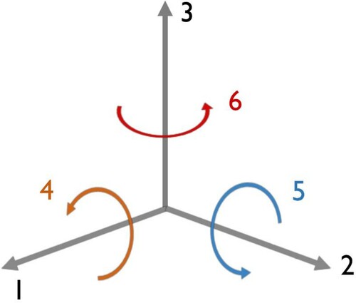
Table 1. Definitions of the piezoelectric coefficients, including their experimental relevance and units.
Figure 2. Three commonly used piezoelectric polymers for practical applications: P(VDF-TrFE), odd-numbered Nylons and PLLA. The sample preparation required in order for each material to exhibit piezoelectricity is also shown, where DR is the draw ratio, T is the drawing temperature and E is the electric field strength of the poling field. *The full piezoelectric tensor of odd-numbered Nylons is scarcely reported.. Given the sample preparation used, the symmetry is assumed to be mm2.
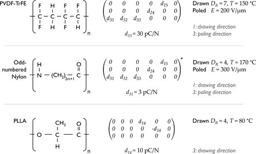
Figure 3. (a) A schematic representation of polymer crystallisation as a result of annealing. Note how that even after crystallisation, the polymer remains isotropic and hence crystallisation in itself is often not sufficient to remove a centre of symmetry. (b) The influence of polymer crystalline fraction on the piezoelectric coefficient of PLLA. Data reproduced with permission from reference [Citation60] . (c) The influence of annealing temperature on the piezoelectric properties of Nylon-11 and Nylon-7. In this instance, annealing has a negative impact, reducing the piezoelectric coefficient. Data reproduced with permission from reference [Citation61] .
![Figure 3. (a) A schematic representation of polymer crystallisation as a result of annealing. Note how that even after crystallisation, the polymer remains isotropic and hence crystallisation in itself is often not sufficient to remove a centre of symmetry. (b) The influence of polymer crystalline fraction on the piezoelectric coefficient of PLLA. Data reproduced with permission from reference [Citation60] . (c) The influence of annealing temperature on the piezoelectric properties of Nylon-11 and Nylon-7. In this instance, annealing has a negative impact, reducing the piezoelectric coefficient. Data reproduced with permission from reference [Citation61] .](/cms/asset/24f6b9bf-d11c-4eb7-be51-fa08b45e1aaf/yimr_a_1915935_f0003_oc.jpg)
Figure 4. (a) A schematic illustration of the effect of drawing on a polymer sample. The material in the drawn region exhibits a significantly higher degree of orientation. The degree of orientation increases with the draw ratio – the ratio of the final and initial sample lengths. (b) The influence of the draw ratio on the piezoelectric coefficients e31 and d31 of Nylon-11 measured at 25°C. The draw ratio has a negligible effect on the d31 coefficient. Drawing is seen to increase e31 due to changes in the mechanical properties of the material. Data reproduced with permission from reference [Citation69] . (c) The influence of the draw ratio on the piezoelectric coefficient of PLLA. A maximum in d14 is observed at a draw ratio of ∼5. Data reproduced with permission from reference [Citation75].
![Figure 4. (a) A schematic illustration of the effect of drawing on a polymer sample. The material in the drawn region exhibits a significantly higher degree of orientation. The degree of orientation increases with the draw ratio – the ratio of the final and initial sample lengths. (b) The influence of the draw ratio on the piezoelectric coefficients e31 and d31 of Nylon-11 measured at 25°C. The draw ratio has a negligible effect on the d31 coefficient. Drawing is seen to increase e31 due to changes in the mechanical properties of the material. Data reproduced with permission from reference [Citation69] . (c) The influence of the draw ratio on the piezoelectric coefficient of PLLA. A maximum in d14 is observed at a draw ratio of ∼5. Data reproduced with permission from reference [Citation75].](/cms/asset/8d34f84c-e145-4123-9467-2e43b2e95a64/yimr_a_1915935_f0004_oc.jpg)
Figure 5. (a) (i) A schematic of an un-poled ferroelectric material. The arrows represent dipole moments. (ii) Poling of a ferroelectric material through the use of attached surface electrodes. (iii) Corona poling of a ferroelectric material. This method does not require electrodes to be attached to the material. (b) The influence of (i) poling time and (ii) poling field on the piezoelectric response of P(VDF-TrFE). Data reproduced from reference [Citation62] under the Creative Commons CC BY license. (c) The influence of (i) poling time and (ii) poling field in the d31 piezoelectric coefficient of Nylon-11. Dielectric breakdown was observed for fields larger than 350 kV/cm. Data reproduced with permission from reference [Citation85] .
![Figure 5. (a) (i) A schematic of an un-poled ferroelectric material. The arrows represent dipole moments. (ii) Poling of a ferroelectric material through the use of attached surface electrodes. (iii) Corona poling of a ferroelectric material. This method does not require electrodes to be attached to the material. (b) The influence of (i) poling time and (ii) poling field on the piezoelectric response of P(VDF-TrFE). Data reproduced from reference [Citation62] under the Creative Commons CC BY license. (c) The influence of (i) poling time and (ii) poling field in the d31 piezoelectric coefficient of Nylon-11. Dielectric breakdown was observed for fields larger than 350 kV/cm. Data reproduced with permission from reference [Citation85] .](/cms/asset/c8130a8a-1e00-4574-a94b-811df343807d/yimr_a_1915935_f0005_oc.jpg)
Figure 6. (a) The piezoelectric coefficient d33 of a PZT/PVDF 0–3 composite as a function of PZT content. All samples were electrically poled for 30 min at 110°C using a field of 10 kV mm−1. Data reproduced with permission from reference [Citation94] . (b) The influence of multi-wall carbon nanotube (MWCNT) content on the β-phase content of PVDF, as measured by wide-angle X-ray diffraction. Data reproduced with permission from reference [Citation95] . (c) A schematic representation of how layered silicate nanoclays, in this instance Lucentite, can nucleate the β-phase in PVDF. Figure adapted with permission from reference [Citation96] .
![Figure 6. (a) The piezoelectric coefficient d33 of a PZT/PVDF 0–3 composite as a function of PZT content. All samples were electrically poled for 30 min at 110°C using a field of 10 kV mm−1. Data reproduced with permission from reference [Citation94] . (b) The influence of multi-wall carbon nanotube (MWCNT) content on the β-phase content of PVDF, as measured by wide-angle X-ray diffraction. Data reproduced with permission from reference [Citation95] . (c) A schematic representation of how layered silicate nanoclays, in this instance Lucentite, can nucleate the β-phase in PVDF. Figure adapted with permission from reference [Citation96] .](/cms/asset/229e8cbe-4017-44da-a104-cae037cbd37c/yimr_a_1915935_f0006_oc.jpg)
Figure 7. (a) (i) The MPB in P(VDF-TrFE), shaded green. The data points represent the transition to the paraelectric phase within the crystalline regions of the polymer. Data were collected by two different material characterisation methods, DMA and DSC. The labels [O, D, P] refer to the state of the crystalline structure: O, ordered; D, disordered; P, pseudo-ordered. (ii) A large increase in d33 is observed around the MPB. Figures reproduced with permission from [Citation110] . (b) A schematic representation of the SSE method used to produce crystalline and aligned films of piezoelectric polymers. Figures adapted with permission from [Citation112] .
![Figure 7. (a) (i) The MPB in P(VDF-TrFE), shaded green. The data points represent the transition to the paraelectric phase within the crystalline regions of the polymer. Data were collected by two different material characterisation methods, DMA and DSC. The labels [O, D, P] refer to the state of the crystalline structure: O, ordered; D, disordered; P, pseudo-ordered. (ii) A large increase in d33 is observed around the MPB. Figures reproduced with permission from [Citation110] . (b) A schematic representation of the SSE method used to produce crystalline and aligned films of piezoelectric polymers. Figures adapted with permission from [Citation112] .](/cms/asset/906368c7-90e4-4103-85a5-7ae00f99f24b/yimr_a_1915935_f0007_oc.jpg)
Figure 8. (a) (i) A schematic of the electrospinning process. Figure reproduced with permission from reference [Citation121] . (ii) Typical polymer nanofibres produced via electrospinning. Image reproduced from reference [Citation122] under the Creative Commons CC BY license. (b) (i) A solution template wetting process to produce PLLA nanowires, shown in part (ii). Figures reproduced from reference [Citation123] under the Creative Commons CC BY license.
![Figure 8. (a) (i) A schematic of the electrospinning process. Figure reproduced with permission from reference [Citation121] . (ii) Typical polymer nanofibres produced via electrospinning. Image reproduced from reference [Citation122] under the Creative Commons CC BY license. (b) (i) A solution template wetting process to produce PLLA nanowires, shown in part (ii). Figures reproduced from reference [Citation123] under the Creative Commons CC BY license.](/cms/asset/85bfe8ec-38eb-46d9-a5c1-bc89b1fe57fa/yimr_a_1915935_f0008_oc.jpg)
Figure 9. (a) A commercially available piezoelectric PVDF sensor. Image credit [Citation155]. (b) A section of a P(VDF-TrFE)-based tactile sensor array. Figure reproduced with permission from reference [Citation157] . (c) (i) An EH device comprised P(VDF-TrFE) nanowires grown by template wetting. (ii) The open-circuit voltage and short-circuit current of this device when subjected to cyclic loading. Figures adapted from reference [Citation145] under the Creative Commons CC BY license. (d) (i) A schematic operating principle of a nanostructured piezoelectric cell culture surface. Compliant piezoelectric nanostructures are deformed by an adherent cell, generating surface charge. (ii) A human dermal fibroblast growing among an array of piezoelectric PLLA nanotubes. Figures reproduced from reference [Citation31] under the Creative Commons CC BY license.
![Figure 9. (a) A commercially available piezoelectric PVDF sensor. Image credit [Citation155]. (b) A section of a P(VDF-TrFE)-based tactile sensor array. Figure reproduced with permission from reference [Citation157] . (c) (i) An EH device comprised P(VDF-TrFE) nanowires grown by template wetting. (ii) The open-circuit voltage and short-circuit current of this device when subjected to cyclic loading. Figures adapted from reference [Citation145] under the Creative Commons CC BY license. (d) (i) A schematic operating principle of a nanostructured piezoelectric cell culture surface. Compliant piezoelectric nanostructures are deformed by an adherent cell, generating surface charge. (ii) A human dermal fibroblast growing among an array of piezoelectric PLLA nanotubes. Figures reproduced from reference [Citation31] under the Creative Commons CC BY license.](/cms/asset/b64a77be-2749-46a2-ad71-689fc49950a6/yimr_a_1915935_f0009_oc.jpg)