
Figures & data
Figure 1. Schematic illustrations of the electrodes arrangements for bulk current measurements (a) and for corona charging of the material sample (b).
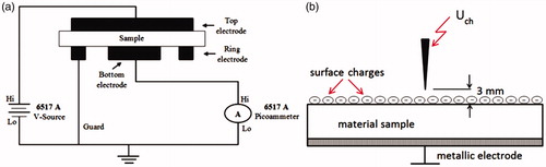
Figure 2. General (a) and top (b) views of the experimental setup. In (b), sample positioning system is shown with charging and scanning setups mounted inside the test vessel. Material sample is placed on the top of plate. Note that the charging needle and the probe are beneath the arm and are facing downwards to the sample.
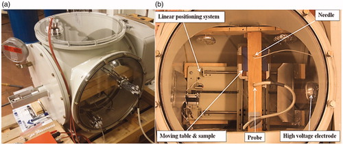
Table 1. Specification of the studied materials.
Table 2. Surface conductivities (at 1 kV), dielectric constants εr(at 50 Hz) and thickness of the samples.
Figure 3. Measured volume currents at room temperature for materials A, B (a) and C, D (b) at different amplitudes of test voltages. The first spike in both the figures corresponds to the application of 300 V, followed by 600, 800, 900, and 1 kV.
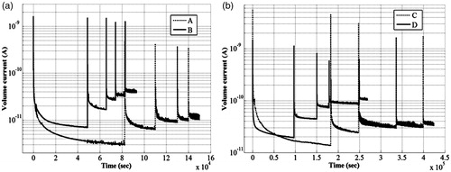
Figure 4. Current density J vs. applied electric field E characteristics for studied materials. The solid and broken lines represent liner fittings with slope 1, the error bars show the standard deviations.
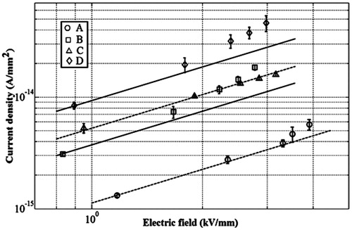
Table 3. Bulk conductivities of the studied materials deduced from the measured volume currents at different amplitudes of DC test voltages.
Figure 5. Normalized surface potential decay characteristics obtained at room temperature for different samples of HTV silicone rubber materials.
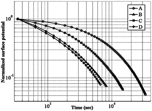
Figure 6. Bulk conductivities of the materials deduced from the measured surface potentials (solid symbols) and obtained from standard measurements (SM) of volume currents. Error bars for SPD are not displayed due to a very weak scatter between the measurements [Citation6].
![Figure 6. Bulk conductivities of the materials deduced from the measured surface potentials (solid symbols) and obtained from standard measurements (SM) of volume currents. Error bars for SPD are not displayed due to a very weak scatter between the measurements [Citation6].](/cms/asset/701a358a-0c38-499d-a71d-9f887494416a/gpac_a_1516369_f0006_b.jpg)
Table 4. Deviations of the values KV obtained from SPD characteristics from the output of standard measurements.