Figures & data
Figure 1. (a) The effects of polymer swelling by water uptake on the nature of the “water wire” within a latent track; (b) explanation of the charge accumulation with subsequent discharge along an obstacle within a water-filled track (Citation3, Citation5, Citation10). The thickness d of the remaining foil segment separating the etched track from the opposite surface is given by d = U/E, with E being the breakthrough field strength – for PET it is 19–160 V/µm.
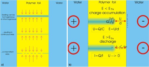
Figure 2. Illustration of the cross-talk of two neighbored spike-emitting SHI ion tracks (Citation3, Citation9). For ∼ 150 nm < λ < ∼2–3 mm, full lateral track-track cross-talk is possible, with λ being the average track-track distance. Optimum cross-talk is obtained for λ being slightly above the minimum distance of 150 nm. For λ < 150 nm, polymer carbonization sets in, resulting in the sample’s destruction. For λ > 2–3 mm, when the time required for full charge synchronization is exceeded, synchronization worsens dramatically (these numbers hold for typically applied potentials U = 1 … 5 V and frequencies around ∼ 1 Hz in the corresponding experiments).
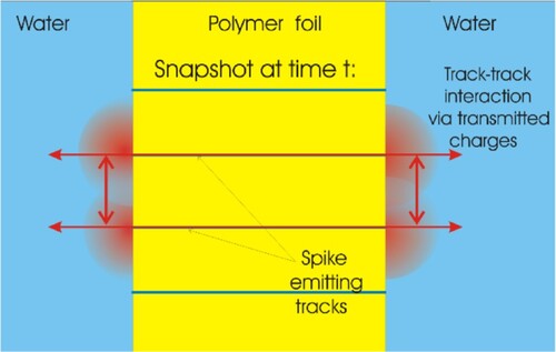
Figure 3. Principle sketch of TCS: a voltage generator (above) feeds sinusoidal signals into the etchant half-vessel (below, left; usually NaOH is used as the etchant). The signal passes the central foil from its cis-side towards its trans-side on the way to the stopper half-vessel on the opposite right (trans) side (usually containing H2O or HCl, to neutralize the etchant more rapidly) The transmitted signals are collected by the “probe” section where the signals are processed and fed into the display and storage unit.
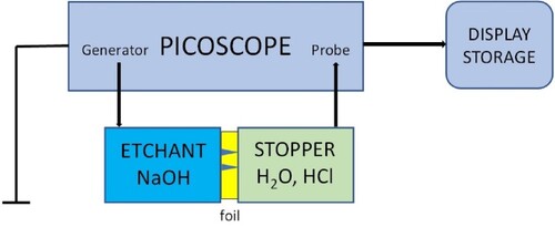
Figure 4. (a) TRIM simulation of the ion distribution (a1), the electronic energy transfer distribution (a2), and the nuclear energy transfer distribution (a3) of 13 MeV O5+ ions impinging into a 12 µm thick PET foil; (b) TRIM simulations of ion trajectories of these ions in lateral view, for 1500 and 15000 ions per spot (for clarity, both simulations are shown in the same figure). Considering that in the experiments a ∼ 1 µm thick microbeam was used, a more realistic graph for the high-fluence example would indicate a damaged area near the trans-side region with a width of about ∼ 3 µm.
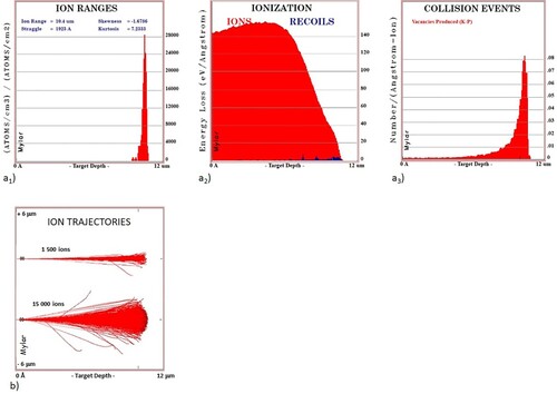
Table 1. Overview of the typical properties of representative SLI-irradiated etched samples that showed spike emission.
Figure 5. Etching protocol of sample CON1, irradiated by 1.2 × 10¹¹ ions/cm−2 (i.e. 3 × 1010 cm−2 ions on 4 neighboring spots of ∼ 1 µm2 each); measurement with ± 1 V AC at 261.2 mHz, applied across the sample in the etching vessel. Display (a) shows a detail of the first protocol, which was taken 9 min after the onset of etching, after which some faint breakthrough current showed up nearly immediately; display (b) starts at 39 min after the beginning of etching. All spectra show numerous different tiny pulses overlaying the basic sinusoidal transmission signal. Spike emission stops abruptly after ∼ 70 min, leaving pure Ohmic transmission currents only. Red sinusoidal curves: applied voltage, blue curves: response of current transmitted across the etched foil.
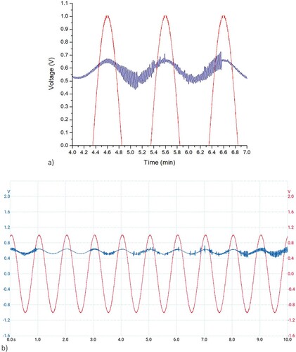
Figure 6. Spike emission properties of sample CON1; (a) the type of spike sequence, in dependence of the etching time, (b) correlation of spike sequence maximum heights with etching time. Added are also the time intervals during which no spike sequences show up, but only occasionally individual single spikes. (c) Correlation of spike sequence widths with etching time. d) Correlation of maximum spike heights and widths. Some faint proportionality might eventually show up, but possibly also different correlations hold.
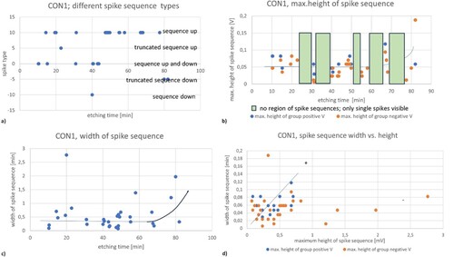
Figure 7. Original measuring protocols of the measured transmission signals for sample CON21. Shown are cut-outs a) from 100.0 to 108.3 min after the onset of etching, and b) from 208,3 to 217.0 min after the onset of etching.
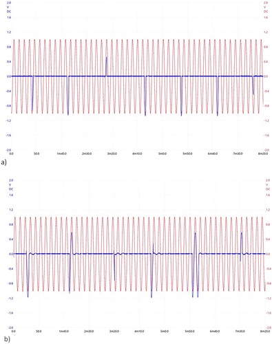
Figure 8. Overview of the physical spike parameters derived from the measurement of sample CON21. Primary correlations: (a) spike heights, (b) spike widths, and (c) the time interval between two successive spikes, as a function of the etching time. Finally, (d) schematically summarizes the emergence of increasingly more complex spike types (y = 10 → 40) and the emergence of short-time Ohmic currents during the progress of etching (y = 0). The value y = 10 describes single mono-modal spikes, y = 20 describes single bi-modal spikes, y = 30 corresponds to single tri-modal spikes, and y = 40 indicates even more complex multi-modal spike structures.
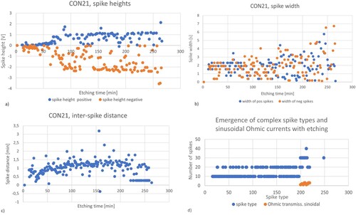
Figure 9. (a) Measuring protocol of sample CON23: (a) from 104,7 to 125 min, and (b) from 125 to 130,3 min. (a) The etchant breakthrough and onset of spike emission (blue) are nearly coincident, covering nearly exclusively only the negative sinusoidal half widths of the applied external voltage (red).
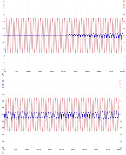
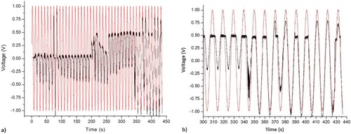
Figure 10. Measuring protocol of sample CON33; (a) overview of all the relevant etching time from 0 to about 450 seconds; Detailed view: (b) from 300 to 450 s. Spike emission (black) covers preferentially the positive sinusoidal half widths of the applied external voltage (red).