
Figures & data
Figure 1. Schematic diagram showing Al/p-Si Schottky diodes with circular Schottky contacts (top surface) and ohmic contact (bottom).
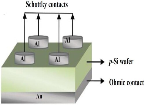
Figure 2. ln(I)-V characteristics of the diodes fabricated on undoped (a) and Fe-doped (b) p-Si prior to irradiation and after irradiation.
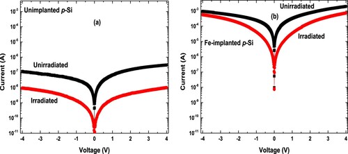
Figure 3. Current ratio () against voltage (V) for undoped and Fe-doped p-Si diode. Inset: Rescaled ΔI against voltage (V) plot for Fe-doped p-Si diode.
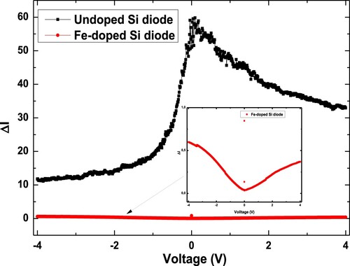
Table 1. The diode parameters for undoped and Fe-doped p-Si diodes prior to and after proton-irradiation.
Figure 4. Forward bias I-V characteristics of the diodes fabricated on undoped (a) and Fe-doped (b) p-Si diode prior to and after irradiation.
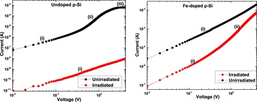
Figure 5. C-V characteristics of the diodes fabricated on undoped (a) and Fe-doped (b) p-Si prior to and after irradiation. Inset: Rescaled C-V characteristics of proton-irradiated p-Si diode.
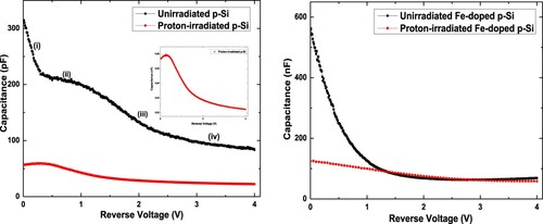
Figure 6. C−2-V characteristics of the diodes fabricated on undoped (a) and Fe-doped (b) p-Si prior to irradiation and after irradiation.
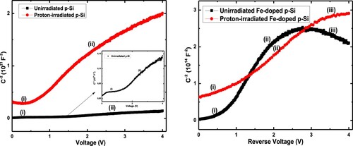
Table 2. The diode parameters for undoped and Fe-doped p-Si diodes prior to and after proton-irradiation evaluated from -V plot.