Figures & data
Figure 1. (a) Conceptual diagram of bolts in automobiles. (b1, b2) the schematic of inserting the TENG sensor into the loose bolt. (c1-c6) the fabrication process of CCTO/PDMS film and CP-TENG device. (d) the picture of gasket with copper foil attached. (e) the picture of gasket with CCTO/PDMS film attached. (f) the SEM image of CCTO/PDMS film surface.
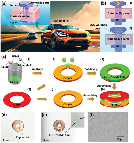
Figure 2. (a) Structural diagram of mechanical system for CP-TENG device. (b) the output signal waveform of Voc and Isc of CP-TENG device. (c1, c2) the working principle of CP-TENG device. The (d) Voc and (e) Isc of CP-TENG under different temperature. (f, g) the influence of CCTO/PDMS film thickness on CP-TENG output performance under different acceleration conditions.
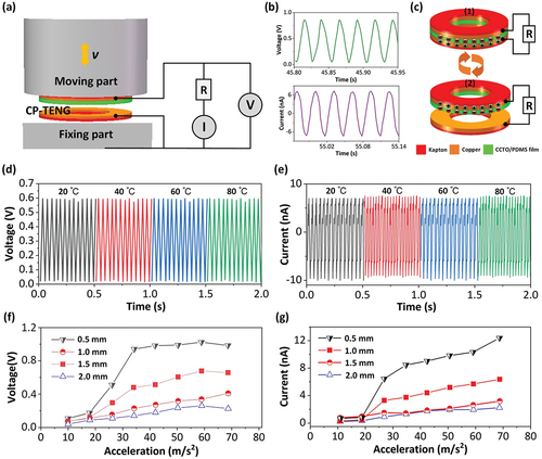
Figure 3. (a) the Voc of CP-TENG under different acceleration. (b) the Isc of CP-TENG under different acceleration. (c, d) the reliability testing of CP-TENG device.
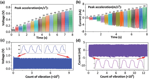
Figure 4. (a) System overview diagram of CP-TENG device for vibration monitoring. (b) the output voltage signal of CP-TENG device during vibration process. (c) the picture of bolt vibration test scenario. (d) the time domain signal and FFT spectrum of the CP-TENG device.
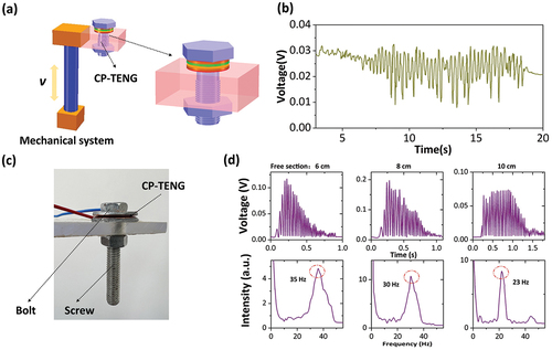
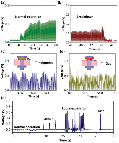
Figure 5. (a) the output voltage signal of CP-TENG under normal operation. (b) the output voltage signal of CP-TENG under breakdown state. The output voltage signal of CP-TENG under (c) compression state and (d) loose state. (e) the output voltage signal of CP-TENG under low-frequency impact conditions.