Figures & data
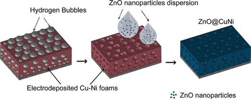
Figure 1. Schematic flow of the synthesis of the ZnO@CuNi hybrid porous layers. From (a) to (b) hydrogen bubble-assisted electrodeposition of porous CuNi MF and from (c) to (d) impregnation of the CuNi scaffold with ZnO NPs suspension.
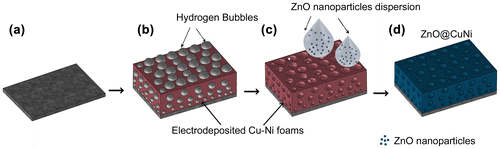
Figure 2. XRD patterns of (a) Cu65Ni35 (red) and ZnO@Cu65Ni35 (black) and (b) Cu80Ni20 (red) and ZnO@Cu80Ni20 (black). Peaks denoted by # and × belong to Cu-rich and Ni-rich phases, respectively. Two diffraction peaks at 33.06° and 34.36° belong to (100) Si and (100) α-Ti crystalline planes, respectively, of the substrate. Abbreviation: au = arbitrary units.
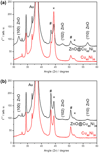
Figure 3. FE-SEM images of (a) the uncoated Cu80Ni20 MF; and the ZnO-coated Cu80Ni20 after (b) three consecutive impregnations (middle coverage) and (c) six consecutive impregnations (final coverage). In each column different magnifications of the three materials are shown.
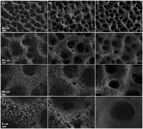
Figure 4. (a) High-resolution TEM image of ZnO@Cu80Ni20 hybrid porous layer; (b) the SAED pattern of the ZnO NPs stacked on the CuNi layer. (c) High-resolution TEM image of an individual ZnO NP. (d) TEM image of as-prepared ZnO nanoparticles; magnified in the inset.
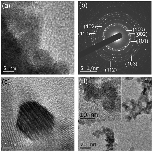
Figure 5. Room temperature hysteresis loops of the (a) Cu80Ni20 and ZnO@Cu80Ni20 and (b) Cu65Ni35 and ZnO@Cu65Ni35 samples.
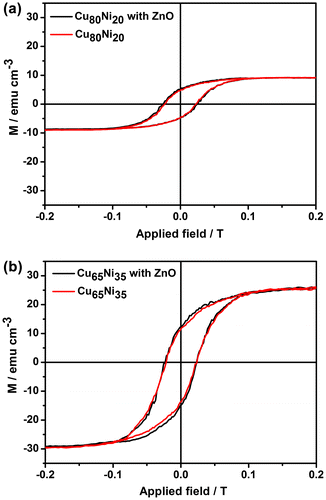
Figure 6. (a) 3D projection images of the hybrid ZnO@Cu80Ni20 nanocomposite isosurface view by Imaris v.6.2.0 software. The 3D representation was obtained from a 50-section stack in steps of 3 μm. CuNi MF shows as gray color (reflection mode) whereas the ZnO component shows as green color (fluorescence). (b) Fluorescence spectrum obtained with the Lambda scan module of CSLM at a 5 nm resolution. Abbreviation: au = arbitrary units.
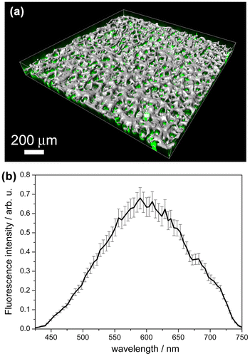
Figure 7. Fluorescence and reflection confocal micrographs (sample area: 621 μm x 621 μm) of the ZnO@Cu80Ni20 hybrid porous layer taken at different sections from the nanocomposite surface up to a total depth of 60 μm. Fluorescence microscopy was employed to visualize ZnO NP (in green). Reflection confocal microscopy was used to visualize the CuNi matrix (in gray).
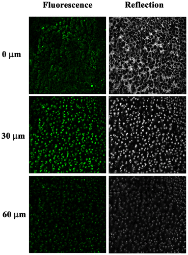
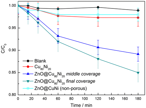
Figure 8. C/C0 plot of the degradation of RhB in the blank, in the presence of Cu80Ni20 MF, and in the presence of ZnO@Cu80Ni20 photocatalysts with middle and final coverages. The RhB degradation profile for ZnO-coated non-porous Cu-rich flat layer is also shown for comparison.