Figures & data
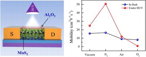
Figure 1. Few-layer MoS2 FET. (a) Optical image of FL-MoS2 flake serving as a conducting channel in the transistor. (b) Optical image of the final device based on the flake shown in (a). The two contacts were used for electrical transport measurements. (c) Raman spectra of the FL-MoS2 pristine (black), O2 treated in the dark (red), N2 treated in the dark (blue), N2 treated under DUV (green), and O2 treated under DUV (pink). (d) Schematic view of the structure of the passivated (10 nm Al2O3 layer) FL-MoS2 FET under DUV illumination. A FL-MoS2 was transferred on a p-doped silicon substrate with a 300-nm-thick SiO2 capping layer. The substrate served as a back gate.
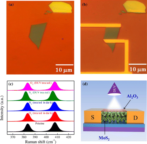
Figure 2. Electrical transport of FL-MoS2 FET before passivation. (a) Transfer characteristics of the FL-MoS2 FET device in the dark. Transfer characteristics were in vacuum, N2, air, and O2 environments. (b) Hysteresis in transfer characteristics of the FL-MoS2 FET device in the dark. Transfer characteristics were obtained under various environmental conditions (vacuum, N2 gas, air, and O2 gas). (c) Transfer characteristics of the FL-MoS2 FET under DUV illumination in vacuum, N2, air, and O2 environments. The power intensity and wavelength of light were 11 mW cm-2 and 220 nm, respectively. (d) Field-effect mobility of the FL-MoS2 FET device in the dark and in the presence of DUV illumination under various environmental conditions.
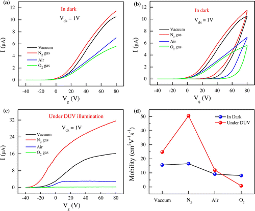
Figure 3. Drain-source characteristics of the device in the dark. The output characteristics (I D-V ds) of the FL-MoS2 FET at fixed V g in (a) vacuum, (b) N2, (c) air, and (d) O2 environments. V g ranges from –20 V to + 60 V with a step of 20 V.
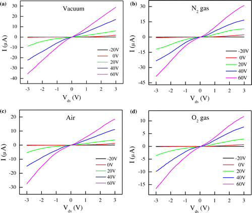
Figure 4. Photocurrent response in various environments. (a) Time-dependent photocurrent response of the device in different environments at V ds = 1 V and V g = 0 V. DUV light was first turned on for 60 s and then turned off for 60 s. (b) Photocurrent saturation of the FL-MoS2 FET in vacuum and N2 gas (left axis and bottom axis), and in air and O2 gas (right axis and top axis) at (V ds = 1 V and V g = 0 V). (c) Saturated photocurrent values in vacuum, N2 gas, air, and O2 gas. (d) Modulation of photocurrent response parameters; maximum responsivity (left axis) and detectivity (right axis) in different environments.
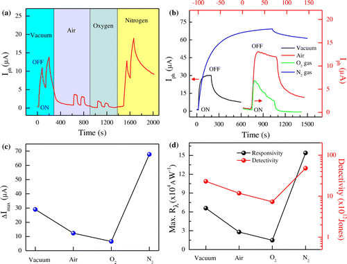
Figure 5. Light detection response. Crucial factors to be calculated in vacuum, N2, air, and O2 for (a) external quantum efficiency and (b) linear dynamic range. The data are obtained from Figure (b), (c), and (d).
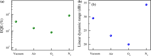
Figure 6. Photocurrent decaying behavior in different environments. Transient property of FL-MoS2 FETs under different conditions and data fitting (red line) with a single exponential equation. (a) Decay of drain current in vacuum. (b) Decay of drain current in N2. The device exhibits a slow decay with a large time constant. (c) Decay of drain current in air and O2. The drain current decays with a small time constant. (d) Relaxation time constants of the device in vacuum, N2, air, and O2.
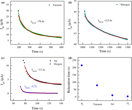
Figure 7. Electrical transport measurements of passivated FL-MoS2 FET. (a) Transfer characteristics of the FL-MoS2 FET device in the dark. Transfer characteristics are measured in vacuum. The linear scale is on the right axis, and the logarithm scale is on the left axis. (b) Hysteresis in transfer characteristics after passivation. The measurements were performed in the dark under different environmental conditions with V g from –60 V to +80 V. (c) Transfer characteristics under DUV illumination. The measurements were carried out in vacuum at V ds = 1 V. The power intensity and wavelength of light were 11 mW cm–2 and 220 nm, respectively. (d) Field–effect mobility of the passivated FL-MoS2 FET device in the dark and under illumination. The measurement was conducted in vacuum.
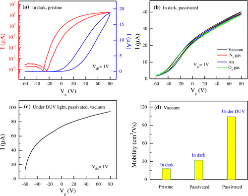
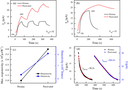
Figure 8. Photocurrent response. (a) Time-dependent photocurrent response of the pristine and passivated devices under vacuum at V ds = 1 V and V g = 0 V. DUV light was initially turned on for 60 s and then turned off for 60 s. (b) Photocurrent saturation of FL-MoS2 FETs in vacuum for the pristine and passivated devices at V ds = 1 V and V g = 0 V. (c) Photocurrent response parameters, including maximum responsivity (left axis) and detectivity (right axis), of the pristine and passivated devices. The data were obtained from Figure (b). (d) Decaying behavior of the pristine and passivated devices when the light was turned off after photocurrent saturation. The red line presents the fitting by a single exponent equation.