Figures & data
Figure 1. SEM images of the (a) as-grown and (b) 14-hour polished film. The as-grown film had clearly defined grains of average size 280 nm. The surface roughness was 44.0 nm RMS in (a) and 1.5 nm RMS in (b).
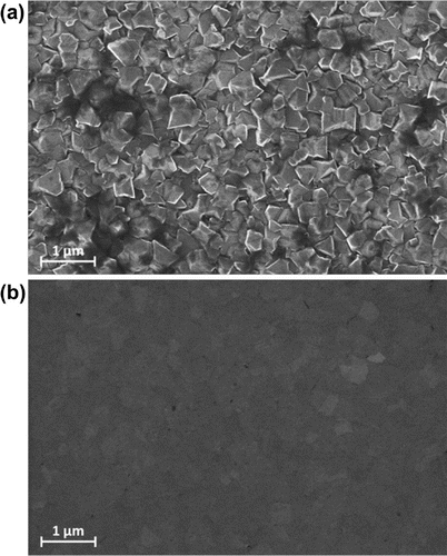
Figure 2. AFM images for the (a) as grown and (b) 14-h polished film. Line traces across the centre of each AFM micrograph are shown in (c) to illustrate the smoothing of the film surface by CMP over time. Inset: the RMS surface roughness as the film is polished.
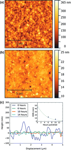
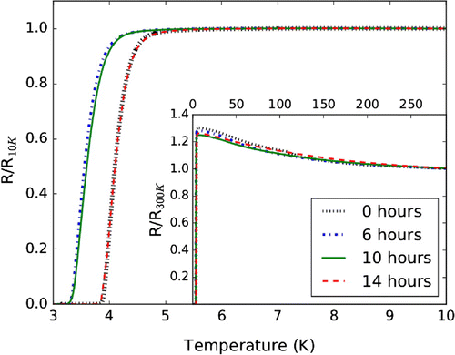
Figure 3. Resistive superconducting transition of the B-NCD film at various stages of polishing. The inset shows the variation of resistance with temperature from 1.6 K to room temperature. The measurement of R(T) for the 14-h polished film is dashed (red) to show that it lies almost exactly on top of the data for the as-grown film (black).