Figures & data
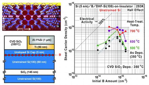
Figure 1. Cross-sectional views for ball-and-stick models of B-doped Si crystals with (a) conventional isolated-atom doping or (b) AL doping for a (100) plane. Blue and red balls are Si and B atoms, respectively. Sticks are covalent bonds for diamond structure.
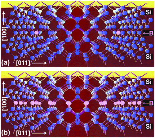
Figure 2. (Top) Plan-view images of carrier transport under lateral electric field in the cases with (a) scattering by isolated ions for the isolated-atom doping and (b) quantum confinement in 2-D ion sheet for the AL doping. Here, the carrier is a hole (‘h+’) in the valence band of Si crystal. (Bottom) Cross-sectional views of isolated or synthetic Coulomb potentials (Φ) affected by the B- ions in the hole-energy-band diagrams.
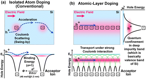
Figure 3. Schematic of our ECR Ar plasma-enhanced CVD system for the B AL-doped Si film formation.
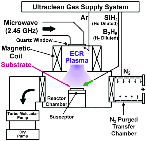
Figure 4. (a) Mask patterns for lithography and (b) schematic cross-sectional structures and typical film thicknesses near the edge of metal contact in the Hall-effect devices on (b-1) the unstrained SOI and (b-2) the 0.8%-tensile-strained SOI. Si cap layer thickness for the Hall-effect devices was fixed at 5 nm.
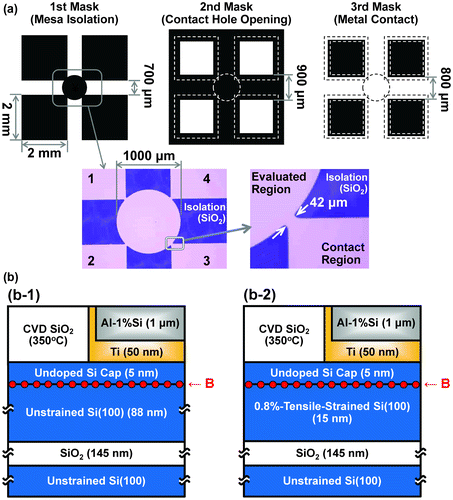
Figure 5. B2H6 reaction time dependence of initial B amount, RHEED patterns and AFM images for the B AL-doped Si films epitaxially grown on (a) the unstrained SOI and (b) the 0.8%-tensile-strained SOI. Root-mean-square (RMS) values of surface roughness are also shown in the AFM images. Si cap layer thickness was fixed at 7 nm.
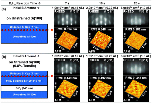
Figure 6. SIMS depth profiles of B and Si concentrations in as-deposited B AL-doped Si films epitaxially grown on (a) unstrained SOI and (b) 0.8%-tensile-strained SOI. B2H6 reaction time was (a-1, b-1) 20 s and (a-2, b-2) 10 s. Si cap layer thickness was fixed at 7 nm. Here, it is confirmed that the B doses, which are integrated values of the B concentration in the regions shown in the figures, are in good agreement with the initial B amounts.
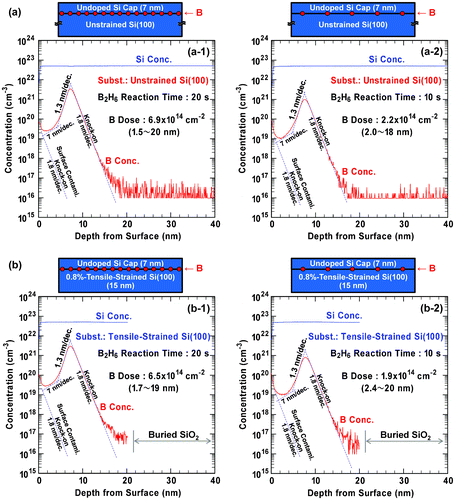
Figure 7. Initial B amount dependence of (a) sheet carrier density and (b) electrical activity of B atom in the B AL-doped Si films on the unstrained SOI (filled marks) and the 0.8%-tensile-strained SOI (open marks). The electrical activity was calculated using the data shown in (a).
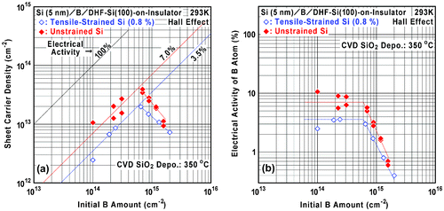
Figure 8. Relationships between excess B amount and sheet carrier loss calculated using the data shown in Figure (a) when a specific electrical activity at lower B amount (7% and 3.5%) and a specific critical B amount (6.0 × 1014 cm−2) are assumed.
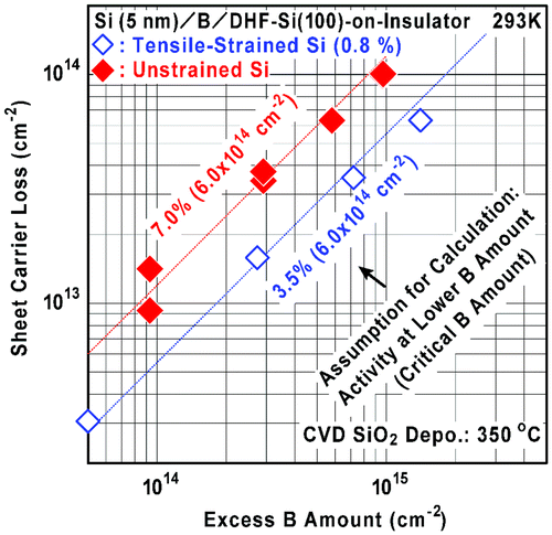
Figure 9. Dependence of Hall mobility (μ) on (a) initial B amount and (b) sheet carrier density (ns) in the B AL-doped Si films on the unstrained SOI (filled marks) and the 0.8%-tensile-strained SOI (open marks).
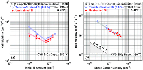
Figure 10. Initial B amount dependence of (a) sheet carrier density and (b) electrical activity of B atom in the B AL-doped Si films on the unstrained SOI at various heat-treatment temperatures for 60 min. The electrical activity was calculated using the data shown in (a).
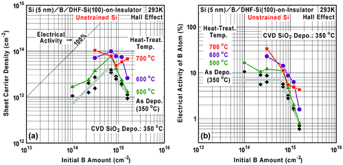
Figure 11. Initial B amount dependence of (a) sheet carrier density and (b) electrical activity of B atom in the B AL-doped Si films on the 0.8%-tensile-strained SOI at various heat-treatment temperatures for 60 min. The electrical activity was calculated using the data shown in (a).
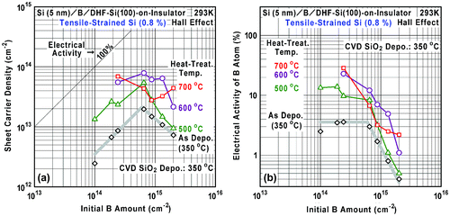
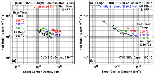
Figure 12. Relationship between sheet carrier density and Hall mobility in the B AL-doped Si films on (a) the unstrained SOI (filled marks) and (b) the 0.8%-tensile-strained SOI (open marks) for various heat-treatment temperatures.