
Figures & data
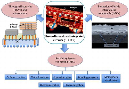
Figure 1. Schematic comparison of three-dimensional (3D) interconnections of (a) stacked die package by wire bonding; (b) package on package by ball grid array (BGA); and (c) wafer and/or dies interconnected with through-silicon via (TSV) [Citation28].
![Figure 1. Schematic comparison of three-dimensional (3D) interconnections of (a) stacked die package by wire bonding; (b) package on package by ball grid array (BGA); and (c) wafer and/or dies interconnected with through-silicon via (TSV) [Citation28].](/cms/asset/13af49c3-cf18-4158-bb01-cf635c4ae649/tsta_a_1364975_f0001_oc.gif)
Figure 2. Synchrotron radiation tomography of 3D ICs test sample with the blue arrows representing the electrical flow during device operation [Citation48].
![Figure 2. Synchrotron radiation tomography of 3D ICs test sample with the blue arrows representing the electrical flow during device operation [Citation48].](/cms/asset/c130ab45-250e-4217-bcec-c2f06f0abf46/tsta_a_1364975_f0002_oc.gif)
Table 1. Different adsorption and penetration energies of M atoms on the a-axis and c-axis of Sn solder [Citation69].
Figure 3. (a) Phase diagram [Citation74] and (b) bonding profile of binary Cu-Sn couple [Citation75].
![Figure 3. (a) Phase diagram [Citation74] and (b) bonding profile of binary Cu-Sn couple [Citation75].](/cms/asset/3d7c1aec-176e-4e71-b80a-b9d68949056b/tsta_a_1364975_f0003_oc.gif)
Figure 4. Scanning electron microscopy (SEM) images of Cu/Sn diffusion coupled with Kirkendall void formation at the Cu3Sn layer (a) without electromigration effect [Citation76] and (b) with electromigration effect [Citation95].
![Figure 4. Scanning electron microscopy (SEM) images of Cu/Sn diffusion coupled with Kirkendall void formation at the Cu3Sn layer (a) without electromigration effect [Citation76] and (b) with electromigration effect [Citation95].](/cms/asset/ae2fc1c8-86d6-48d5-baef-3867a21e55d1/tsta_a_1364975_f0004_oc.gif)
Figure 5. EBSD orientation maps (TD) of Cu-Sn IMCs (RD: reverse direction and TD: transverse direction) [Citation96].
![Figure 5. EBSD orientation maps (TD) of Cu-Sn IMCs (RD: reverse direction and TD: transverse direction) [Citation96].](/cms/asset/5aa551fe-9c99-43d0-bddd-0c5daa865b01/tsta_a_1364975_f0005_oc.gif)
Table 2. Analysis of total IMC thickness with respect to different aging times, constant atmospheric condition and constant temperature for each solder joint.
Figure 6. Schematic diagram of two β-Sn grain interconnects separated by grain boundaries with different electron flows: (a) forward direction and (b) reverse direction [Citation112].
![Figure 6. Schematic diagram of two β-Sn grain interconnects separated by grain boundaries with different electron flows: (a) forward direction and (b) reverse direction [Citation112].](/cms/asset/65424ba9-1d78-4e77-b21f-20eed5fe2241/tsta_a_1364975_f0006_oc.gif)
Table 3. Asymmetric growth of IMCs on the cold and hot sides.
Figure 7. (a) Schematic illustration of the asymmetric growth of IMCs during thermomigration and (b) SEM images of the asymmetric growth of Ni3Sn4 IMCs under thermomigration conditions at the hot end (190°C) and cold end (100°C) for 150 h [Citation113].
![Figure 7. (a) Schematic illustration of the asymmetric growth of IMCs during thermomigration and (b) SEM images of the asymmetric growth of Ni3Sn4 IMCs under thermomigration conditions at the hot end (190°C) and cold end (100°C) for 150 h [Citation113].](/cms/asset/f64ea39d-69d2-42d1-8622-dc6b87ba227f/tsta_a_1364975_f0007_oc.gif)