Figures & data
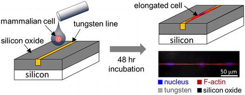
Figure 1. Schematic drawings depict the specimen fabrication process. The thin titanium (Ti) seed layer is shown in yellow, silicon oxide in blue, and the tungsten (W) layer in red. Note the final specimen surfaces are smooth and flat without protrusions.
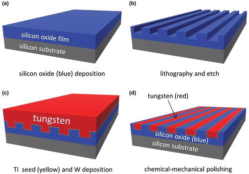
Figure 2. Schematic drawing of a cell on tungsten/silicon oxide patterned comb structure and their orientation parameters.
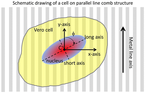
Figure 3. (a) SEM micrograph of a 2 μm tungsten line comb structures and two isolated tungsten lines with same width. (b) Micrograph shows a close-up image of parallel tungsten/silicon oxide line structures with line widths of 2 μm.
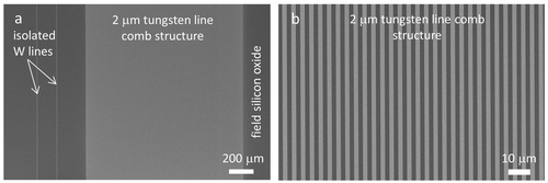
Table 1. Data summary of tungsten/silicon oxide comb structures: physical dimensions, inspected areas, number of cells inspected, % population of cells with 10° > ϕ > −10° and 20° > ϕ > −20° of the metal line axis. The culture media initial cell concentration used was 2 × 10⁵ cells/mL. Data spreads correspond to one standard deviation.
Figure 4. (a) Cross-sectional SEM images of dense metal patterns with 0.5 μm wide tungsten lines with 1.5 μm spacing. (b) A high magnification cross-sectional SEM image of a 0.5 μm wide tungsten line.
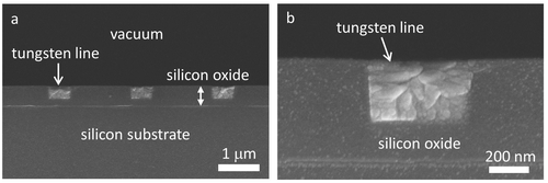
Figure 5. (a) and (b) Confocal fluorescence micrographs of Vero cells on the bare silicon substrate. (c) A non-dividing cell elongated on a 0.18 μm wide isolated tungsten line. (d) and (e) Micrographs of a dividing cell at low and high magnification, respectively. (f) Two non-dividing cells and one dividing cell attached to a 2 μm wide isolated tungsten line. (g) High-magnification image of a dividing nucleus. (h) and (i) Micrographs of cells attached to a 10 μm wide isolated tungsten line at low and high magnifications, respectively. Cell nuclei were labeled with DAPI and appear blue. F-actin microfilaments were stained with red fluorescent phalloidin conjugate and appear red. All cells were incubated for 24 hours.
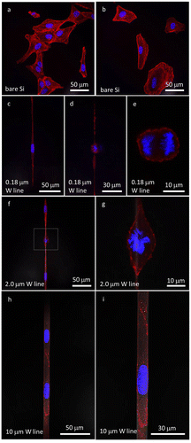
Table 2. Average long and short axis lengths of cell nuclei incubated on bare silicon, polished blanket tungsten, and polished silicon oxide for 24 hours. Data spreads correspond to one standard deviation.
Figure 6. SEM micrographs (70o tilted) of Vero cells on 10 μm comb structures with incubation time between 0.5 and 49.25 hours.
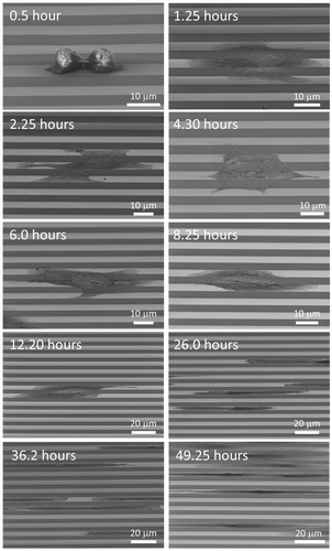
Figure 7. Cell orientation distributions on 10 μm comb structures when cultured in baseline (containing 10% FBS), OptiPRO (serum free), and OptiPRO + 10% FBS media. The number of cells inspected (n) on the specimens are displayed in the legend.
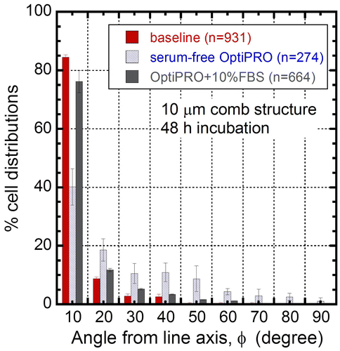
Figure 8. SEM micrographs revealing changes in cell adhesion characteristics with tungsten line widths of (a) 0.18 μm, (b) 10 μm, (c) 50 μm, and (d) 100 μm. Tungsten line width and silicon oxide spacing in the comb structure are identical in each image.
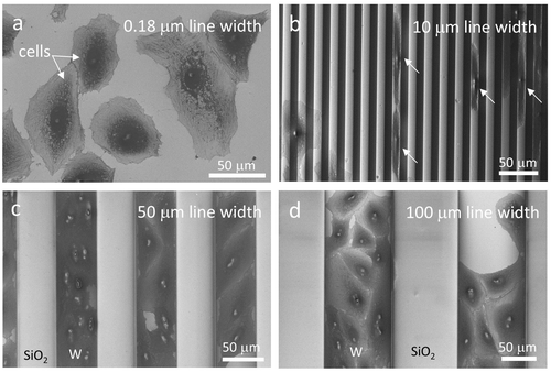
Figure 9. (a) Plots of percent cell distribution as a function of the angle between the nuclei long axis and the metal line axis. They include results from bare silicon substrate, polished field tungsten, polished field silicon oxide, and comb structures with line widths in the range of 0.18 μm to 100 μm. The number of cells inspected in each comb structures (n) is included in each chart. Each bar represents a 10° bin of deviations from the line axis (either +/−), i.e. a cell with a nucleus major axis of −24o would be counted in the second bin from the left in each plot. Error bars correspond to one standard deviation of three independent cell populations. The initial cell concentration of the culture media was 2 ×10⁵ cells/mL. (b) Plot of cell orientation distributions as a function line width.
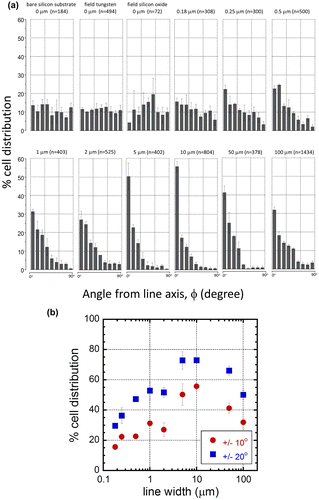
Figure 10. (a) Representative SEM micrographs of a comb structure with 10 μm wide tungsten lines and 90 μm spacing. (b) Plot of percentage cell distribution as a function of angles between the major axis of the nuclei and the metal axis. Parameter n is the total number of cells sampled.
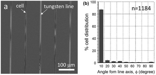
Figure 11. (a) Observed cell morphologies on different surfaces (polished field tungsten area – field W; bare silicon – bare Si; polished silicon oxide – polish oxide; surface with isolated 2 μm line – 2 μm W line; surface with 0.18 μm tungsten isolated line – 0.18 μm W line) with a superimposed simulated comb pattern used in the calculation of coverage in (c). (b) Schematic drawing indicating cell orientation relative to the simulated comb structure; the pink circle and yellow diamond represent cells with random and elongated shapes, respectively. (c) Cell-tungsten coverage of cells plotted as a function of simulated tungsten line widths (w).
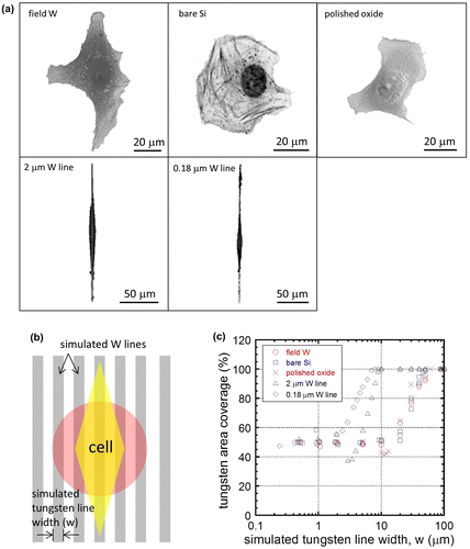
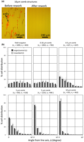
Figure 12. (a) Typical optical micrographs of the same 10 μm comb structures before and after the rework process to remove QT-35 cells. (b) Adherent cell orientations on virgin/control (c) and reworked (r) specimens. nc and nr represent the numbers of cells characterized within each comb structure on virgin and reworked specimens. Error bars correspond to one standard deviation. Initial cell concentration of the culture media is 0.5 × 10⁵ cells/mL.