Figures & data
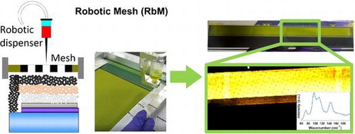
Figure 1. Schematic representation of deposition methods for perovskite precursor solutions on C-PSCs. (a) drop method (b) robotic mesh method (RbM).
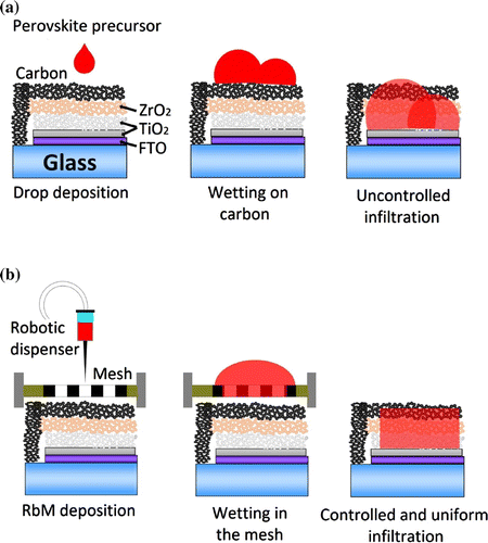
Figure 2. (a) Deposition of solution over a mesoporous stack, in sequence: a
solution is deposited as continuous line over a carbon stripe; the liquid reorganises in drops; and the characteristic dot-like pattern is shown from the back side through the glass. (b) Change in contact angle of a
in DMF solution on a mesoporous carbon layer over time. Inset, the droplet on carbon at time 0.
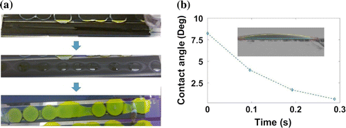
Figure 3. Devices prepared by (a) drop or (b) RbM deposition. On the top, small devices (1 ) before and after conversion of
; at the bottom, long stripes (10
) after conversion with a blow-up of a selected area.
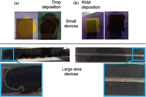
Figure 4. Comparison of 10 cm samples prepared by drop and RbM deposition prior to conversion into MAPI. (a) Visual appearance of samples obtained using a camera. (b) Raman map obtained at around 96 . A measured
Raman signal is also shown. The peaks at 73, 96, and 110
belong to
, the peak at 144
to
. The colour scale is shown for the two maps.
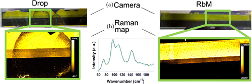
Figure 5. An XRD false colour map of 10 cm samples prepared by drop and RbM following conversion to MAPI. The relative intensities of the peaks at 12.7 and 14.2
were used to map the
and MAPI phases, respectively. Each square of the false colour map is 1
of the sample area. Colour scale for each phase is shown. The diffractograms of each point are shown for drop and RbM samples.
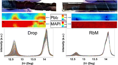
Figure 6. Statistical analysis of JV data comparing Ctrl and RbM cells. Best devices derived from this data set exhibit PCE values of 10.9 and 9.8%, respectively, for Ctrl and RbM cells.
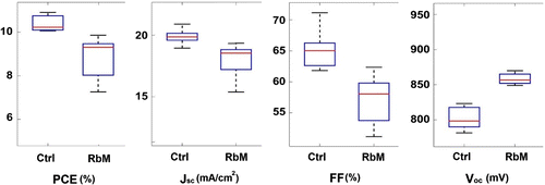
Table 1. Average performance of Ctrl and RbM cells. PCE stands for power conversion efficiency, FF for filling factor, for open-circuit voltage, and Hyst for the ratio of PCEs measured in forward and reverse scans.
Figure 7. Representative example of JV curves of devices in forward (from low to high voltage) and reverse scan with stabilised current and PCE measured for 40 s. EQE spectra of the devices are shown.
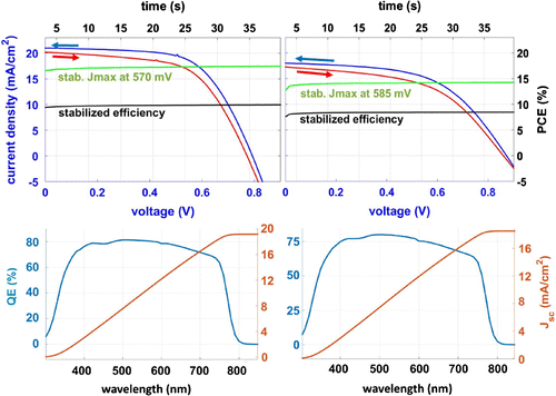
Figure 8. (a) EIS Nyquist plot at different light intensity of a representative cell per each deposition method. (b left) Intensity dependence of the ; (b right) recombination resistance dependence of the applied voltage,
.
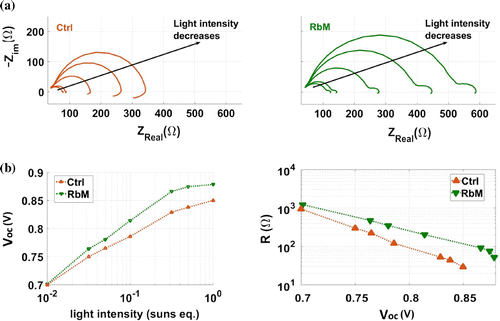
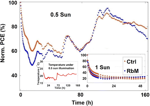
Figure 9. Normalised PCE of both Ctrl and RbM cells over time during continuous illumination from white LED, at 0.5 and 1 equivalent sun; temperature profile under 0.5 sun during the test. At 0.5 sun, the drop in PCE is not as severe as under 1 sun and a nearly complete recovery is observed after few days. The PCE profile under 0.5 sun follows the temperature profile.