
Figures & data
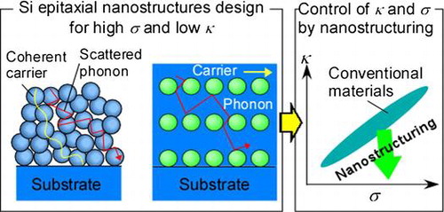
Figure 1. (a) Importance of independent control of thermal and electric conductivities by nanostructuring in thermoelectric material study. (b) Examples of thin film thermoelectric generators.
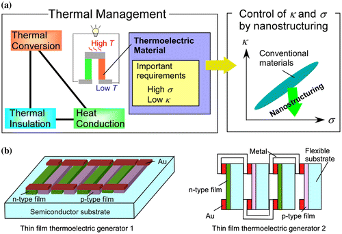
Figure 2. Proposed nanostructures for independent control of thermal and electric conductivities. (a) structure of connected Si NDs and (b) Si film containing NDs.
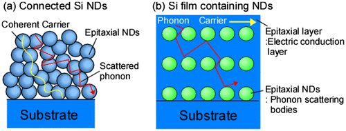
Figure 3. Ultrathin Si oxide film technique for epitaxial growth of NDs.
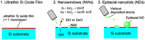
Figure 4. (a) Cross-sectional high-resolution transmission electron microscopy image and (b) the schematic of Ge NDs epitaxially grown on Si substrate. Reprinted (adapted) with permission from Nakamura et al. [Citation49]. © 2011 American Chemical Society.
![Figure 4. (a) Cross-sectional high-resolution transmission electron microscopy image and (b) the schematic of Ge NDs epitaxially grown on Si substrate. Reprinted (adapted) with permission from Nakamura et al. [Citation49]. © 2011 American Chemical Society.](/cms/asset/e91af7ee-7bee-4f41-ae2d-e0ce34346ed4/tsta_a_1413918_f0004_oc.gif)
Figure 5. Scanning tunneling microscopy images of NDs formed by ultrathin Si oxide film technique. (a) 5-monolayer (ML) Ge0.85Sn0.15 NDs, (b) 15-ML GaSb NDs, (c) 12-ML β-FeSi2 NDs, and (d) Ge ND array.
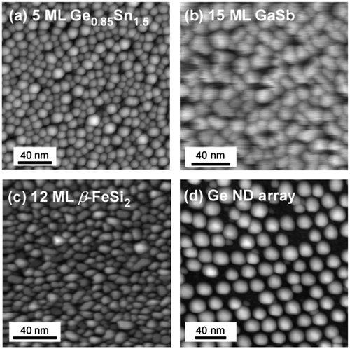
Figure 6. Scanning tunneling spectroscopy of Ge NDs with (a) small (2.0 nm) and (b) large (5.6 nm) diameters. Reprinted (adapted) with permission from Nakamura et al. [Citation36]. © 2005 American Institute of Physics.
![Figure 6. Scanning tunneling spectroscopy of Ge NDs with (a) small (2.0 nm) and (b) large (5.6 nm) diameters. Reprinted (adapted) with permission from Nakamura et al. [Citation36]. © 2005 American Institute of Physics.](/cms/asset/2a44f091-31a7-469e-8727-db8ef7388547/tsta_a_1413918_f0006_oc.gif)
Figure 7. Cross-sectional HRTEM image of Ge films/Si formed by nanocontact epitaxy. (a) low and (b) high magnification. Reprinted (adapted) with permission from Nakamura et al. [Citation49]. © 2011 American Chemical Society.
![Figure 7. Cross-sectional HRTEM image of Ge films/Si formed by nanocontact epitaxy. (a) low and (b) high magnification. Reprinted (adapted) with permission from Nakamura et al. [Citation49]. © 2011 American Chemical Society.](/cms/asset/e99beceb-2d07-47dc-879e-2b24e978bf53/tsta_a_1413918_f0007_oc.gif)
Figure 8. RHEED patterns of (a) clean Si surfaces, (b) ultrathin Si oxide film, and (c) and (d) Si nanodots ((c) 1st and (d) 7th cycles).
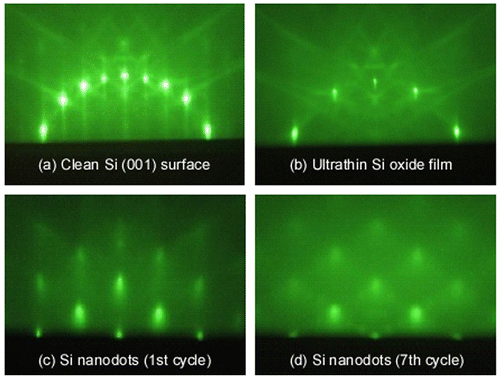
Figure 9. (a) HRTEM image of connected epitaxial Si NDs and (b) FFT pattern of Si NDs. Reprinted with permission from Nakamura et al. [Citation30], (c) 2015 Elsevier.
![Figure 9. (a) HRTEM image of connected epitaxial Si NDs and (b) FFT pattern of Si NDs. Reprinted with permission from Nakamura et al. [Citation30], (c) 2015 Elsevier.](/cms/asset/8a78a941-2d20-409a-a8b7-2faf7ff7c88f/tsta_a_1413918_f0009_b.gif)
Figure 10. (a) Thermal conductivity of connected epitaxial Si NDs with the preceding Si nanostructure results, (b) enlarged graph of (a). Reprinted with permission from Nakamura et al. [Citation30], © 2015 Elsevier.
![Figure 10. (a) Thermal conductivity of connected epitaxial Si NDs with the preceding Si nanostructure results, (b) enlarged graph of (a). Reprinted with permission from Nakamura et al. [Citation30], © 2015 Elsevier.](/cms/asset/c8a88fb1-0c29-432e-8b9f-de484022c2f5/tsta_a_1413918_f0010_oc.gif)
Figure 11. TRC of connected epitaxial Si NDs and the calculated TRC of Si/SiO2 superlattice. Reprinted with permission from Nakamura et al. [Citation30], © 2015 Elsevier.
![Figure 11. TRC of connected epitaxial Si NDs and the calculated TRC of Si/SiO2 superlattice. Reprinted with permission from Nakamura et al. [Citation30], © 2015 Elsevier.](/cms/asset/31b91a9c-9f83-4f7f-8378-9232a180e748/tsta_a_1413918_f0011_oc.gif)
Figure 12. RHEED patterns of (a) ultrathin Si oxide film, (b)Ge NDs formed in 1st cycle process, (c) Si layers, (d) the ultrathin Si oxide film on Si layer, (e) and (f) Ge NDs formed in (e) 3th and (f) 8th cycles.
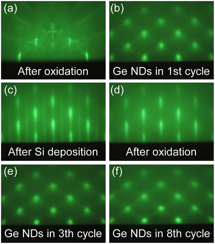
Figure 13. Cross-sectional HRTEM image of Si films containing Ge NDs (stacking structure of Ge NDs/Si) formed by ultrathin SiO2 film technique (a) and high magnification image near the interface (b). The inset in (a) is a schematic of Si films containing Ge NDs. Reprinted (adapted) with permission from Yamasaka et al. [Citation7]. © 2015 Springer Nature.
![Figure 13. Cross-sectional HRTEM image of Si films containing Ge NDs (stacking structure of Ge NDs/Si) formed by ultrathin SiO2 film technique (a) and high magnification image near the interface (b). The inset in (a) is a schematic of Si films containing Ge NDs. Reprinted (adapted) with permission from Yamasaka et al. [Citation7]. © 2015 Springer Nature.](/cms/asset/39a0435a-fcb4-475f-921f-1c782a10e51e/tsta_a_1413918_f0013_oc.gif)
Figure 14. Thermal conductivity of Si films containing Ge NDs (stacking structure of Ge NDs/Si) with the preceding results. Reprinted (adapted) with permission from Yamasaka et al. [Citation7]. © 2015 Springer Nature.
![Figure 14. Thermal conductivity of Si films containing Ge NDs (stacking structure of Ge NDs/Si) with the preceding results. Reprinted (adapted) with permission from Yamasaka et al. [Citation7]. © 2015 Springer Nature.](/cms/asset/2bec0e6f-00e5-4991-91a2-998eefab8528/tsta_a_1413918_f0014_oc.gif)
Figure 15. The Ge ND size dependence of the TRC in Si films containing Ge NDs with the rough tendency of phonon scattering probability (the dashed line) (a) and the schematics of phonon scattering and transports (b). Reprinted (adapted) with permission from Yamasaka et al. [Citation7]. © 2015 Springer Nature.
![Figure 15. The Ge ND size dependence of the TRC in Si films containing Ge NDs with the rough tendency of phonon scattering probability (the dashed line) (a) and the schematics of phonon scattering and transports (b). Reprinted (adapted) with permission from Yamasaka et al. [Citation7]. © 2015 Springer Nature.](/cms/asset/4caf9ffc-c851-460a-96ef-e66415e85ecd/tsta_a_1413918_f0015_oc.gif)
Figure 16. The electrical properties of Si films containing Ge NDs. P-doped (n-type) (a) and B-doped (p-type) samples (b). Results of epitaxial Si films in literatures are also shown for references (open square, circle, triangle marks are from Refs. [Citation68–70], respectively). Calculated lines for bulk Si are also taken from Ref. [Citation67]. Dotted line in (a) is an eye-guide.
![Figure 16. The electrical properties of Si films containing Ge NDs. P-doped (n-type) (a) and B-doped (p-type) samples (b). Results of epitaxial Si films in literatures are also shown for references (open square, circle, triangle marks are from Refs. [Citation68–70], respectively). Calculated lines for bulk Si are also taken from Ref. [Citation67]. Dotted line in (a) is an eye-guide.](/cms/asset/2b2bc228-fcde-4da3-913d-f3c5e7bb2ade/tsta_a_1413918_f0016_oc.gif)