Figures & data
Figure 1. Classification of carbon allotropes derived from graphene.
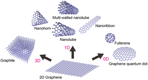
Figure 2. Methodologies for synthesizing GQDs through top-down routes. Reproduced with permission from [Citation42–49]. Copyright 2010, 2012, 2013, Wiley-VCH. Copyright 2009, 2012, 2013, American Chemical Society. Copyright 2011, Macmillan Publishers Limited.
![Figure 2. Methodologies for synthesizing GQDs through top-down routes. Reproduced with permission from [Citation42–49]. Copyright 2010, 2012, 2013, Wiley-VCH. Copyright 2009, 2012, 2013, American Chemical Society. Copyright 2011, Macmillan Publishers Limited.](/cms/asset/9cc2c7e6-9ace-497a-9179-4f61bead485a/tsta_a_1422224_f0002_oc.gif)
Figure 3. Changes in the optical properties of GQDs-based on size and surface state. (a) UV–vis spectra of GQDs A, B, and C, correspond to synthesis reaction temperatures of 120, 100, and 80 °C, respectively. (b) PL spectra of GQDs with different emission color. Reproduced with permission from [Citation47]. Copyright 2012, American Chemical Society. (c) Size-dependent PL spectra excited at 325 nm for 5–35 nm GQDs in deionized (DI) water. Inset: different colors of luminescence from GQDs depending on their average size for three typical GQDs of 12, 17, and 22 nm. Reproduced with permission from [Citation56]. Copyright 2012, American Chemical Society. (d) Bandgap changes for GQDs, m-GQDs, and r-GQDs. Reproduced with permission from [Citation59]. Copyright 2012, Wiley-VCH. (e) Normalized PL (black lines) and PL excitation (red lines) spectra from aqueous amino-functionalized GQDs (afGQDs) solutions prepared under different conditions. (f) PL image of an aqueous afGQDs solution under excitation from a blue light-emitting diode (LED) (410 nm). Reproduced with permission from [Citation57]. Copyright 2015, Royal Society of Chemistry.
![Figure 3. Changes in the optical properties of GQDs-based on size and surface state. (a) UV–vis spectra of GQDs A, B, and C, correspond to synthesis reaction temperatures of 120, 100, and 80 °C, respectively. (b) PL spectra of GQDs with different emission color. Reproduced with permission from [Citation47]. Copyright 2012, American Chemical Society. (c) Size-dependent PL spectra excited at 325 nm for 5–35 nm GQDs in deionized (DI) water. Inset: different colors of luminescence from GQDs depending on their average size for three typical GQDs of 12, 17, and 22 nm. Reproduced with permission from [Citation56]. Copyright 2012, American Chemical Society. (d) Bandgap changes for GQDs, m-GQDs, and r-GQDs. Reproduced with permission from [Citation59]. Copyright 2012, Wiley-VCH. (e) Normalized PL (black lines) and PL excitation (red lines) spectra from aqueous amino-functionalized GQDs (afGQDs) solutions prepared under different conditions. (f) PL image of an aqueous afGQDs solution under excitation from a blue light-emitting diode (LED) (410 nm). Reproduced with permission from [Citation57]. Copyright 2015, Royal Society of Chemistry.](/cms/asset/15c277fc-28ac-4996-8c1e-391f44a5604a/tsta_a_1422224_f0003_oc.gif)
Figure 4. Modulation of the optical properties in GQDs through chemical functionalization alone. Energy levels and PL for nitrogen-functionalized graphene quantum dots (NGQDs). (a) Predicted energy level diagrams for graphene with different functional groups. (b) Measured energy level diagram for NGQDs. (c) PL image of NGQDs in aqueous solution excited using a UV lamp (365 nm): (i) Azo-GQDs; (ii) NH2-GQDs; (iii) OPD-GQDs; and (iv) DAN-GQDs. (d) Corresponding normalized PL spectra (excited at 380 nm) from aqueous dispersions of NGQDs. Reproduced with permission from [Citation62]. Copyright 2016, Wiley-VCH.
![Figure 4. Modulation of the optical properties in GQDs through chemical functionalization alone. Energy levels and PL for nitrogen-functionalized graphene quantum dots (NGQDs). (a) Predicted energy level diagrams for graphene with different functional groups. (b) Measured energy level diagram for NGQDs. (c) PL image of NGQDs in aqueous solution excited using a UV lamp (365 nm): (i) Azo-GQDs; (ii) NH2-GQDs; (iii) OPD-GQDs; and (iv) DAN-GQDs. (d) Corresponding normalized PL spectra (excited at 380 nm) from aqueous dispersions of NGQDs. Reproduced with permission from [Citation62]. Copyright 2016, Wiley-VCH.](/cms/asset/01b28735-065d-47f3-9cc4-a061076cf89f/tsta_a_1422224_f0004_oc.gif)
Table 1. Classification of substituent effects on.
Figure 5. GQDs-based photodetectors. (a) Schematic illustration of the configuration for photoconductive measurements of GQDs with asymmetric electrodes. (b) Time response of the device under pulsed 254 or 302 nm DUV light (42 μW cm−2). Reproduced with permission from [Citation63]. Copyright 2015, American Chemical Society. (c) Schematic of the energy level alignment for the photodoping effect. (d) Photoresponsivity vs. optical irradiation power (laser wavelengths of 254–940 nm) for the DAN-GQD/BN-NS@GFET hybrid PD. Reproduced with permission from [Citation54]. Copyright 2016, Royal Society of Chemistry. (e) Schematic representation of the NMe2-GQD@GFET hybrid PD. PEN stands for polyethylene naphthalate (f) Spectral response (left axis) from the NMe2-GQD@GFET PD (V SD = 0.1 V, V G = 0 V, 0.06 μW cm−2). The solid orange area (right axis) represents the UV–vis absorption spectrum of a NMe2-GQD solution. Reproduced with permission from [Citation64]. Copyright 2017, Macmillan Publishers Limited.
![Figure 5. GQDs-based photodetectors. (a) Schematic illustration of the configuration for photoconductive measurements of GQDs with asymmetric electrodes. (b) Time response of the device under pulsed 254 or 302 nm DUV light (42 μW cm−2). Reproduced with permission from [Citation63]. Copyright 2015, American Chemical Society. (c) Schematic of the energy level alignment for the photodoping effect. (d) Photoresponsivity vs. optical irradiation power (laser wavelengths of 254–940 nm) for the DAN-GQD/BN-NS@GFET hybrid PD. Reproduced with permission from [Citation54]. Copyright 2016, Royal Society of Chemistry. (e) Schematic representation of the NMe2-GQD@GFET hybrid PD. PEN stands for polyethylene naphthalate (f) Spectral response (left axis) from the NMe2-GQD@GFET PD (V SD = 0.1 V, V G = 0 V, 0.06 μW cm−2). The solid orange area (right axis) represents the UV–vis absorption spectrum of a NMe2-GQD solution. Reproduced with permission from [Citation64]. Copyright 2017, Macmillan Publishers Limited.](/cms/asset/113d5a98-bc8c-43e9-a59d-daca1af9b8ff/tsta_a_1422224_f0005_oc.gif)
Figure 6. GQDs-based organic photovoltaic devices. (a) J–V characteristics of the devices based on aniline (ANI) and GQDs with different GQDs content and on aniline and graphene sheets (GSs, under optimized conditions) annealed at 160 °C for 10 min, under AM 1.5G 100 mW illumination. Reproduced with permission from [Citation67]. Copyright 2011, American Chemical Society. (b) Schematics of the ITO/PEDOT:PSS/P3HT:GQDs/Al device containing indium tin oxide (ITO), poly(ethylene dioxythiophene)–polystyrene sulfonic acid (PEDOT:PSS) and poly(3-hexylthiophene-2,5-diyl) (P3HT). (c) J–V characteristic curves for the ITO/PEDOT:PSS/P3HT/Al, ITO/PEDOT:PSS/P3HT:GQDs/Al and ITO/PEDOT:PSS/P3HT:GQDs/Al devices after annealing at 140 °C for 10 min. Reproduced with permission from [Citation68]. Copyright 2011, Wiley-VCH.
![Figure 6. GQDs-based organic photovoltaic devices. (a) J–V characteristics of the devices based on aniline (ANI) and GQDs with different GQDs content and on aniline and graphene sheets (GSs, under optimized conditions) annealed at 160 °C for 10 min, under AM 1.5G 100 mW illumination. Reproduced with permission from [Citation67]. Copyright 2011, American Chemical Society. (b) Schematics of the ITO/PEDOT:PSS/P3HT:GQDs/Al device containing indium tin oxide (ITO), poly(ethylene dioxythiophene)–polystyrene sulfonic acid (PEDOT:PSS) and poly(3-hexylthiophene-2,5-diyl) (P3HT). (c) J–V characteristic curves for the ITO/PEDOT:PSS/P3HT/Al, ITO/PEDOT:PSS/P3HT:GQDs/Al and ITO/PEDOT:PSS/P3HT:GQDs/Al devices after annealing at 140 °C for 10 min. Reproduced with permission from [Citation68]. Copyright 2011, Wiley-VCH.](/cms/asset/02363312-4fc0-45fe-aba0-ef61b345adfa/tsta_a_1422224_f0006_oc.gif)
Figure 7. GQDs-based LEDs. (a) Schematic of organic LEDs (OLED) employing GQDs. GraHIL and TPBI (1, 3, 5-tri(phenyl-2-benzimidazolyl)-benzene) are hole and electron transporting layers, respectively. (b) Photograph of white-light emission from an OLED employing 10 nm GQDs. (c) Normalized PL intensity of a set of OLEDs at a fixed bias (13 V). Reproduced with permission from [Citation69]. (d) Schematic illustration of the GQD-LEDs structure and the corresponding band diagram. (e) Electroluminescence image of GQD-LEDs consisting of five emitting areas. (f) Luminous efficiencies and emission spectra of the devices. Copyright 2014, American Chemical Society. Reproduced with permission from [Citation70]. Copyright 2014, Wiley-VCH.
![Figure 7. GQDs-based LEDs. (a) Schematic of organic LEDs (OLED) employing GQDs. GraHIL and TPBI (1, 3, 5-tri(phenyl-2-benzimidazolyl)-benzene) are hole and electron transporting layers, respectively. (b) Photograph of white-light emission from an OLED employing 10 nm GQDs. (c) Normalized PL intensity of a set of OLEDs at a fixed bias (13 V). Reproduced with permission from [Citation69]. (d) Schematic illustration of the GQD-LEDs structure and the corresponding band diagram. (e) Electroluminescence image of GQD-LEDs consisting of five emitting areas. (f) Luminous efficiencies and emission spectra of the devices. Copyright 2014, American Chemical Society. Reproduced with permission from [Citation70]. Copyright 2014, Wiley-VCH.](/cms/asset/182e9f5c-0d2a-45cd-bd8b-3fd14ace70cd/tsta_a_1422224_f0007_oc.gif)
Figure 8. Schematic illustrations of the structures of Zintl binary silicides: (a) CaSi2 and (b) AlB2 type structure. The yellow-colored balls are silicon atoms.
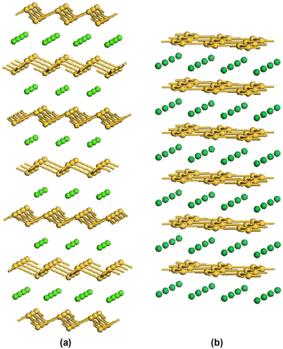
Figure 9. Structure of layered polysilane (SiH)n.
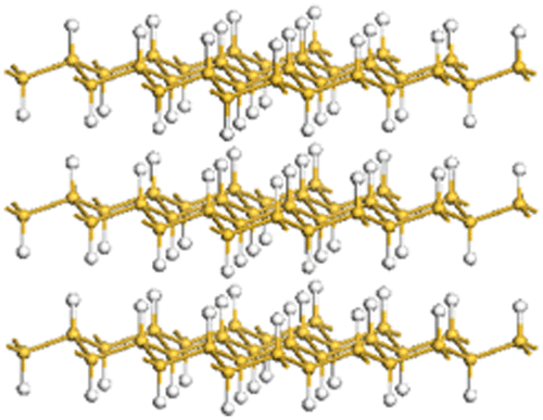
Figure 10. (a) AFM image of the water-adapted silicane and (b) A height profile taken along the white line. (c) Schematic illustration of the water-adapted silicane. (d) Atomically resolved AFM image. Reprinted with permission from [Citation79]. Copyright 2006 Wiley-VCH.
![Figure 10. (a) AFM image of the water-adapted silicane and (b) A height profile taken along the white line. (c) Schematic illustration of the water-adapted silicane. (d) Atomically resolved AFM image. Reprinted with permission from [Citation79]. Copyright 2006 Wiley-VCH.](/cms/asset/7fe32da3-41e8-45c1-b69d-c22be0fea9c3/tsta_a_1422224_f0010_oc.gif)
Figure 11. (a) Stacking properties of amino-modified silicanes. (b) AFM image, a photograph showing the PL of a Ph-silicane solution, and the schematic model of Ph-silicane.
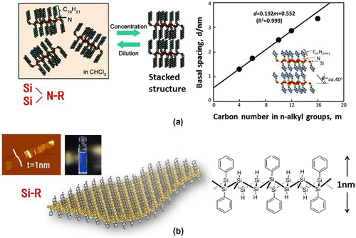
Table 2. Calculated band gap of silicane functionalized with different molecular groups.
Figure 12. Optimized structures of (a) naphthyl and (b) anthracyl-functionalized silicane.
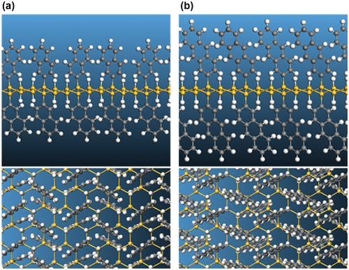
Figure 13. Electron localization function (ELF) plot of the naphthyl-modified silicane.
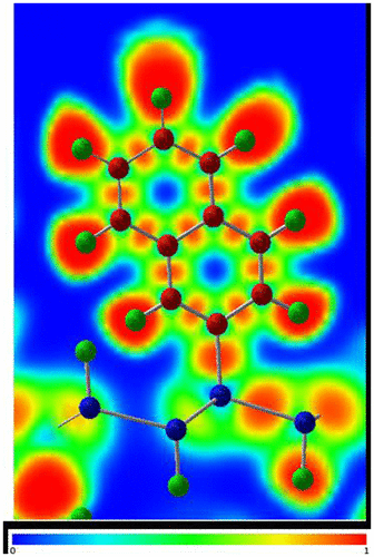
Figure 14. Band structure of the (a) naphthyl and (b) anthracyl-modified silicene.
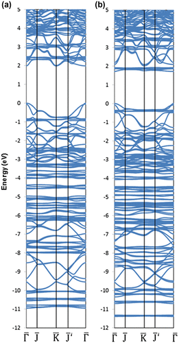
Figure 15. (a) Potential energy of Si confined in a slit pore as a function of temperature (Inset: 2D RMSD of Si over 10 ps). (b) and (c) Top and side views, respectively, of bilayer honeycomb silicene (BHS) obtained in the MD simulation by Morishita et al. [Citation124]. Copyright (2008) The American Physical Society.
![Figure 15. (a) Potential energy of Si confined in a slit pore as a function of temperature (Inset: 2D RMSD of Si over 10 ps). (b) and (c) Top and side views, respectively, of bilayer honeycomb silicene (BHS) obtained in the MD simulation by Morishita et al. [Citation124]. Copyright (2008) The American Physical Society.](/cms/asset/2c244c01-0b50-49f7-975a-bf40b888c8e4/tsta_a_1422224_f0015_oc.gif)
Figure 16. Band dispersion relations for (a) pristine BHS and (b) P-doped BHS (all the outermost Si atoms are substituted by P, thereby no dangling bond exists) [Citation134]. Copyright (2010) The American Physical Society.
![Figure 16. Band dispersion relations for (a) pristine BHS and (b) P-doped BHS (all the outermost Si atoms are substituted by P, thereby no dangling bond exists) [Citation134]. Copyright (2010) The American Physical Society.](/cms/asset/9a6fc6e6-3d1c-41b6-b270-fbc82f1bbe5e/tsta_a_1422224_f0016_b.gif)
Figure 17. Atomic configurations for (a) re-BLS and (b) w-BLS.
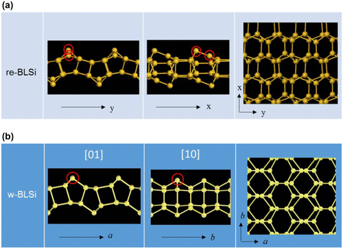
Figure 18. Schematic illustration of the crystal structure of CaSi2 and its reconstruction to w-BLSi.
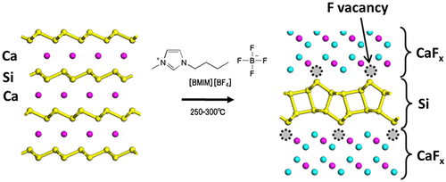
Figure 19. (a) Cross-sectional back-scatter scanning electron microscopy image of the crystal grain, including a CaSi2F x compound. (b) Electron probe micro-analysis along the red arrow in (a). (c–f) STEM-EDX elemental mapping results of the CaSi2F2 composition region. (f) Overlay of Si, Ca, and F mapping. (g) HAADF-STEM image of the STEM-EDX elemental mapping area. Copyright (2016) by the Nature Publishing Group.
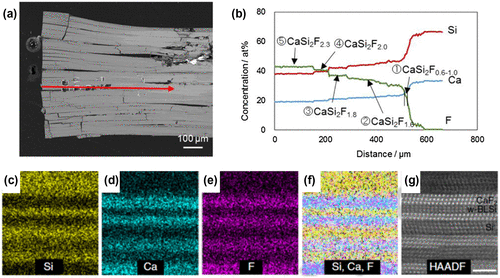
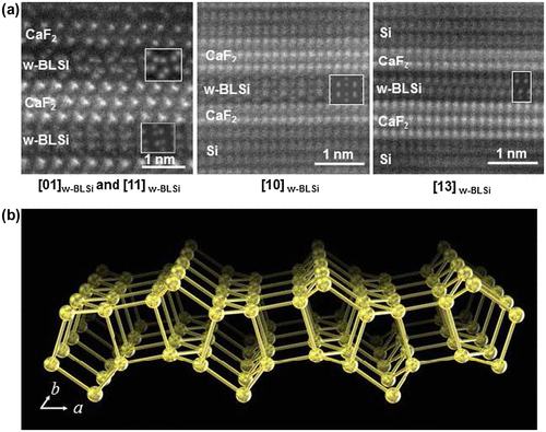
Figure 20. (a) HAADF-STEM images taken along three crystallographic directions and the corresponding simulation (insets) for w-BLSi. (b) Schematic of the w-BLSi atomic structure. Copyright (2016) by the Nature Publishing Group.