Figures & data
Figure 1. SEM images of film deposited using optimised growth parameters at different growth temperatures: (a) 432 °C; (b) 472 °C.
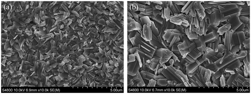
Figure 2. Sn-S phase diagram taken from Ref. [Citation17].
![Figure 2. Sn-S phase diagram taken from Ref. [Citation17].](/cms/asset/f0b3e974-5a72-487e-948f-d30f7dd4174e/tsta_a_1428478_f0002_b.gif)
Table 1. Atomic weight (at. %) composition determined by EDX for films deposited using different S/Sn precursor partial pressure ratios, [S/Sn]i.
Figure 3. Absorption spectra of films deposited at different [S/Sn]i at a growth temperature of 470 °C.
![Figure 3. Absorption spectra of films deposited at different [S/Sn]i at a growth temperature of 470 °C.](/cms/asset/20f7bef5-a96c-4677-a610-e121ed7b86da/tsta_a_1428478_f0003_oc.gif)
Figure 4. Band gap calculation of films deposited at different [S/Sn]i using absorption coefficient × energy squared versus energy, (αE)2 vs. E, for direct () transitions and the square route of absorption coefficient × energy versus energy, (αE)1/2 vs. E, for indirect (
) transitions (inset).
![Figure 4. Band gap calculation of films deposited at different [S/Sn]i using absorption coefficient × energy squared versus energy, (αE)2 vs. E, for direct (Egd) transitions and the square route of absorption coefficient × energy versus energy, (αE)1/2 vs. E, for indirect (Egi) transitions (inset).](/cms/asset/e3245957-4c7d-4df7-ae91-43ce51dfbf09/tsta_a_1428478_f0004_oc.gif)
Figure 5. XRD of films deposited at 470 °C using different [S/Sn]i equal to 5.4, 6.2 and 8.0, which showed cross-over of SnS 1:1 stoichiometry determined from EDX measurements.
![Figure 5. XRD of films deposited at 470 °C using different [S/Sn]i equal to 5.4, 6.2 and 8.0, which showed cross-over of SnS 1:1 stoichiometry determined from EDX measurements.](/cms/asset/9c692710-ea13-4bb7-b563-16240c48ff3e/tsta_a_1428478_f0005_oc.gif)
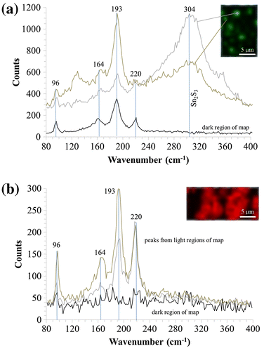
Figure 6. Raman spectroscopy of different film regions for SnS samples deposited at optimised growth parameters on (a) ITO mapped at a 304 cm−1 frequency and (b) Mo mapped at a 193 cm−1 frequency.