Figures & data
Figure 1. Evolution of Pd0.25Ag0.75 nanoparticles (NPs, total thickness 15 nm) on sapphire (0 0 0 1) with annealing temperature between 400 and 900 °C. (a) Schematic of Pd/Ag bilayer deposition. (b)–(g) Schematics of surface phenomena and corresponding AFM top-views of 5 × 5 μm2 in (b-1)–(e-2). Insets show the 3D side-views and line profiles of typical regions. (f) RMS roughness (Rq), surface area ratio (SAR) and (g) EDS counts with respect to the temperature.
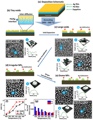
Figure 2. (a)–(c) SEM images of alloy NPs, annealed between 700 and 900 °C for 120 s with 15 nm total thickness. (d)–(f) Average height, diameter and density of the alloy NPs. (g) Reflectance spectra of Pd-Ag alloy NPs on sapphire (0 0 0 1). (h) Raman spectra of A1g vibration mode at ~417 cm−1 of each sample. (i) Average reflectance, (j) Raman intensity, and (k) Raman peak shift with respect to the temperature.
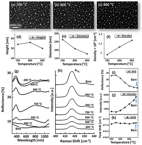
Figure 3. Fabrication of alloy NPs on sapphire (0 0 0 1) with bilayer composition Pd0.5Ag0.5 and 15 nm total thickness, annealed between 400 and 900 °C for 120 s. (a)–(f) AFM top-views of 5 × 5 μm2. (a-1)–(f-1) 3D side-views of typical structures in (a)–(f) and cross-sectional line profiles. (g)–(i) Rq, SAR and EDS count summary with respect to the temperature.
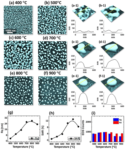
Figure 4. Pd0.75Ag0.25 NPs on sapphire (0 0 0 1) annealed between 400 and 900 °C for 120 s with 15 nm total thickness. (a)–(f) AFM top-views of 5 × 5 μm2. (a-1)–(f-1) Cross-sectional line profiles. (g) Rq, (h) SAR and (i) EDS count with respect to the temperature variation.
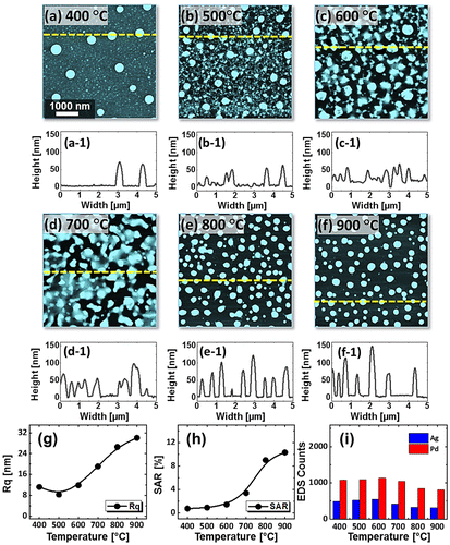
Figure 5. SEM images of Pd-Ag alloy NPs fabricated between 700 and 900 °C with the compositions Pd0.5Ag0.5 in (a)–(c) and Pd0.75Ag0.25 in (d)–(f). (g)–(h) Reflectance spectra of the alloy NPs with distinct composition as labeled. (g-1)–(h-1) Average reflectance of corresponding sets in (g) and (h) with respect to the temperature.
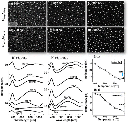
Figure 6. Evolution of dome-shaped Pd0.25Ag0.75 NPs on sapphire (0 0 0 1), with a thickness between 1 and 30 nm, annealed at 850 °C for 120 s. AFM top-views are 1 × 1 μm2 in (a), (b) and 3 × 3 μm2 in (c)–(i). (i-1) AFM side-view and line profile of a typical dome-shaped alloy NPs. (j)–(k) Rq and SAR with respect to thickness.
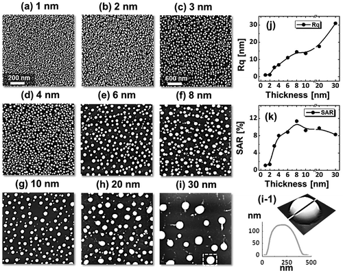
Figure 7. (a) Diameter and (b) height distribution histogram of alloy NPs shown in Figure . (c)–(e) Summary plots of average, height, diameter, density with ~±5% error.
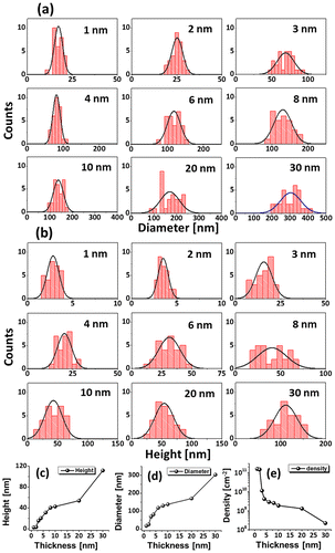
Figure 8. Spherical alloy NPs fabricated at 850 °C for 120 s with 30 nm total thickness for distinct bilayers compositions. SEM images of alloy NPs for (a) Pd0.25Ag0.75, (b) Pd0.5Ag0.5, and (c) Pd0.75Ag0.25 composition. (c-1) Pd-Ag phase map of the alloy NPs in (c). (c-2) Separate Pd and Ag phase maps and EDS line profiles of a selected NP in (c). (c-3) Substrate (Al and O) elemental phase map. (c-4) EDS spectra of the sample showing O, Al, Pd, and Ag peaks. (c-5) 3D top-view of Pd-Ag combined phase map.
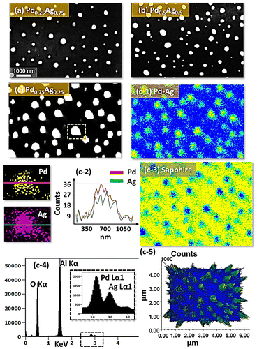
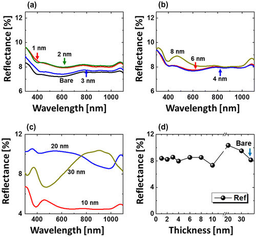
Figure 9. Reflectance spectra of the alloy NPs fabricated at 850 °C for 120 s with composition Pd0.25Ag0.75 and total thickness variation (a) 1–3 nm, (b) 4–8 nm, and (c) 10–30 nm. (d) Average reflectance with respect to thickness.