Figures & data
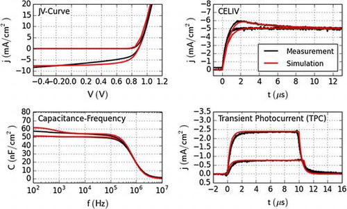
Figure 1. (a) Device structure of the ‘base’ case used in this study. LUMO and HOMO stand for lowest unoccupied and highest occupied molecular orbitals, respectively. (b) Simulation parameters of the ‘base’ case. Full simulation parameters of all cases are listed in the supplemental information (SI).
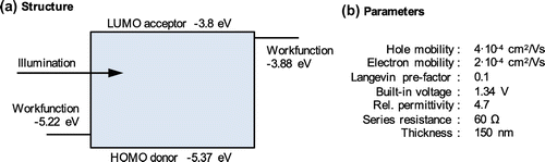
Table 1. Definition of 11 cases of solar cells.
Figure 2. JV-curve simulations for all cases defined in Table . (f) The bar-plot shows the fill-factor of all simulated cases. All the described cases impact the fill-factor. It is difficult to identify a specific physical effect if a JV-curve has a low fill-factor.
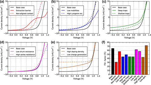
Figure 3. Dark JV-curve simulations for all cases in Table . (f) Dark ideality factors are extracted using Equation (Equation2(2)
(2) ).
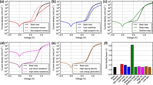
Figure 4. Simulation of the open-circuit voltage dependent on the light intensity for all cases in Table . (f) Light ideality factors obtained from the simulation results – an average is used.
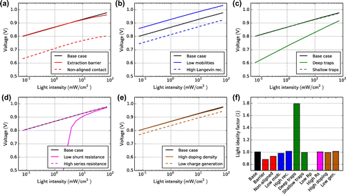
Figure 5. Schematic illustration of a photo-CELIV experiment. The linearly increasing voltage extracts charge carriers and leads to a peak (j max) in current. The charge carrier mobility is calculated using t max.
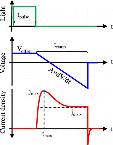
Figure 6. Dark-CELIV simulations of all cases in Table . The ramp starts at t = 0 with a ramp rate of 171 V/ms. (f) The bar plot shows the extracted charge carrier density.
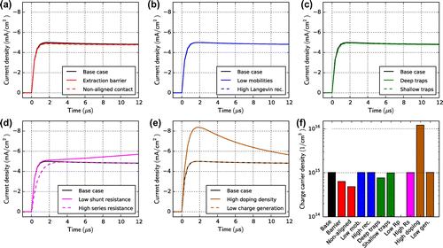
Figure 7. Photo-CELIV simulations for all cases in Table . The light is turned off at t = 0 and the voltage ramp starts at t = 0 with a ramp rate of 100 V/ms. The voltage offset prior the ramp is set such that the current is zero at t < 0. (f) The bar plot shows the charge carrier mobility calculated from the peak position (t
max) using Equation (Equation9(9)
(9) ). The grey lines indicate the electron mobility used as simulation input.
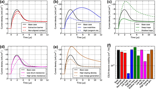
Figure 8. OCVD simulations for all cases in Table . The light is turned off at t = 0. The grey line indicates the analytic solution (Equation (Equation11(11)
(11) )) assuming homogeneous charge densities and purely bimolecular recombination.
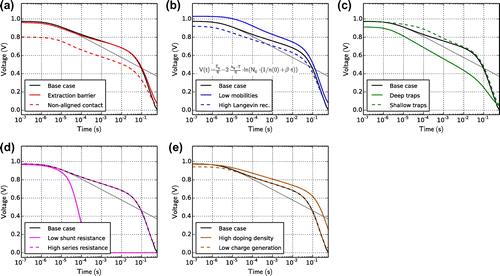
Figure 9. Calculation of the thermal emission of charge carriers from the density of states. (a) The dashed line is the density of states with square-root dependence above the band edge and exponential dependence inside the band. The solid lines represent the charge carrier distributions at different times. The LUMO-level is located at 0 eV, positive energy values reach into the band-gap. (b) Same as in (a) but for a Gaussian DOS. (c) Calculated currents from carrier emission of (a) and (b) including analytical fits according to Equations (Equation14(14)
(14) ) and (Equation16
(16)
(16) ).
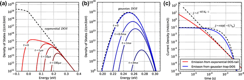
Figure 10. DLTS simulations for all cases in Table . The voltage is 0 V for t < 0. At t = 0 the voltage jumps to −5 V. (f) DLTS simulations of case ‘shallow traps’ at different temperatures (solid lines). The dashed lines are exponential fits according to Equation (Equation14(14)
(14) ).
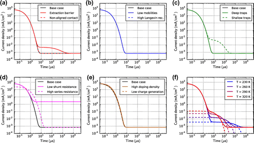
Figure 11. Transient photocurrent simulations for all cases in Table . At t = 0 the illumination is turned on. At t = 15 μs the illumination is turned off. The applied voltage is 0 V. The current is normalized by the current at 15 μs.
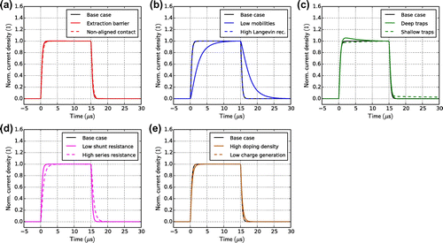
Figure 12. Charge extraction simulations for varied light intensity (and thus V
oc) for all cases defined in Table . The current is integrated over time according to Equation (Equation17(17)
(17) ) to obtain the charge carrier density (the charge on the capacitance is subtracted). The light intensity is varied by five orders of magnitude. The grey-line is the theoretical V
oc for n = p in a zero-dimensional model. (f) Extracted charge carrier density at the highest light intensity. Grey lines represent the effective amount of photogenerated charge at open-circuit obtained from the simulated charge carrier profiles.
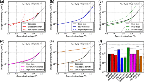
Figure 13. Impedance simulations for all cases in Table . The capacitance C is calculated according to Equation (Equation20(20)
(20) ). The offset-voltage is 0 and offset-light is turned on. The dashed grey line represents the geometric capacitance.
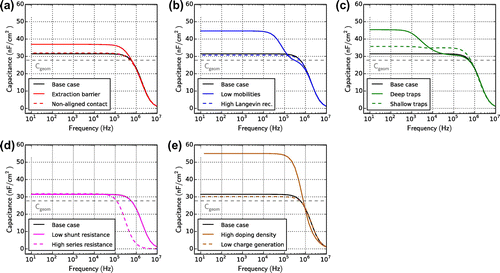
Figure 14. Capacitance-voltage simulations for all cases in Table without offset illumination. The capacitance C is calculated according to Equation (Equation20(20)
(20) ). The frequency is kept constant at 10 kHz. (f) Voltage where the capacitance reaches a maximum.
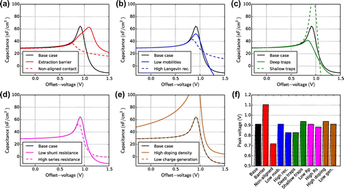
Figure 15. IMPS simulations for all cases in Table with low offset light intensity (3.6 mW/cm2). The offset voltage is zero. (f) IMPS transport time-constant calculated according to Equation (Equation26(26)
(26) ).
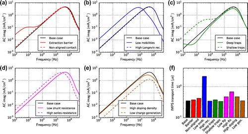
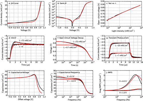
Figure 16. Measurements of an organic PCDTBT:PC70BM solar cell (black) and drift-diffusion simulation results (red) from a global fit. (a) JV-curve under illumination (L = 72 mW/cm2). (b) dark JV-curve. (c) Open-circuit voltage for varied light intensity. (d) Dark-CELIV (L = 0) and photo-CELIV (L = 72 mW/cm2) with ramp rate 100 V/ms. Light is turned off at t = 0. (f) Open-circuit voltage decay for two light intensities. Light is turned off at t = 0. (g) Transient photocurrent for two light intensities. Light is turned on at t = 0 and turned off at t = 10 μs. (h) Impedance spectroscopy at 10 kHz with varied offset-voltage. (i) Impedance spectroscopy at constant voltage with varied frequency. (j) Intensity-modulated photocurrent spectroscopy (IMPS) with constant offset voltage.