Figures & data
Figure 1. Device configuration of standard (a) mesoporous and (b) planar perovskite solar cells. (c) Schematic representation of phenomena limiting the light-harvesting efficiency in planar perovskite solar cells. (d) Optical constant n and k of a typical CH3NH3PbI3 perovskite. (e) Optical absorbance A = 1 − exp(4πk/λ) of perovskite material with different propagation depths.
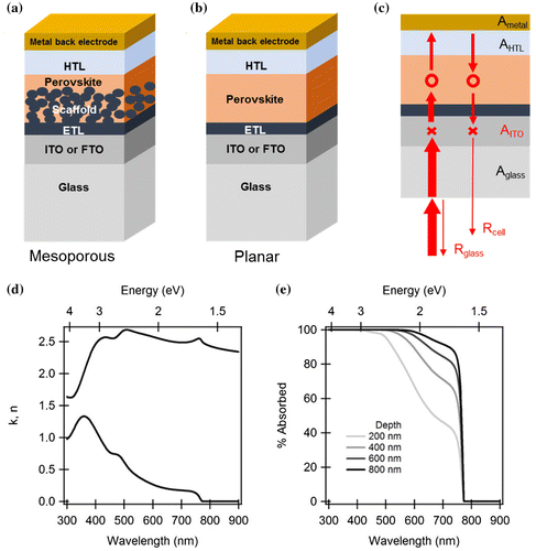
Figure 2. Working principle of ARCs: (a) solar cell without ARC, (b) with layered ARC (destructive interferences), (c) with graded ARC, (d) with wavelength-scale structured ARC.
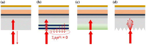
Figure 3. (a) Schematic representation of the solar cell structure including nanocone assembly ARC and (b) the EQE enhancement due to the reduced reflection loss. Adapted with permission from Tavakoli et al., ACS Nano 2015;9(10):10287. © 2015 American Chemical Society. (c) Calculation of the electric field intensity in a perovskite solar cell showing the light focusing capability of the ARC. Adapted with permission from Peer et al., Opt. Express. 2017;25(9):287886. © 2017 Optical Society of America. The image shows the field map inside the fluorine-doped tin oxide (FTO), TiO2 and perovskite layers (schematized as inset). The light impinges from the top onto the front glass surface where the ARC stands (not seen on the image). Nodes of field intensity can be seen in the FTO with their field distribution extending into the perovskite. (d) Calculation of the electric field intensity in the glass substrate of a solar cell including a micropyramid-based ARC showing the oblique propagation of light due to scattering by the surface texture (IMPS stands for inverted micro-pyramidal structure). Reproduced with permission from Dudem et al., J. Mater. Chem. A. 2016;4: 7573. © 2016 Royal Society of Chemistry.
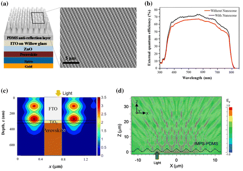
Table 1. Photovoltaic parameters of perovskite solar cells with (‘ARC’) and without (‘Ref’) an anti-reflection coating placed at the air/glass interface of the cell.
Figure 4. (a) Structure of a photonic structure-based cell. The ETL consists of a porous vertical photonic structure (PC stands for photonic crystal) alternating SiO2:TiO2 and TiO2 layers (b). Spectra of the reflectance (solid lines: measurements, dashed lines: calculations; vertically offset for clarity) and calculated wavelength-dependent in-depth distribution of the electric field intensity in the solar cell for two different configurations of the vertical photonic structure (different thicknesses for the SiO2:TiO2 and TiO2 layers). Changing this configuration changes the reflectance spectrum and thus the colour of the cell (in this figure, one has an orange aspect, the other one a blue-green aspect), as well as the in-depth distribution of the electric field. Reproduced with permission from Zhang et al., Nano Lett. 2015;15: 1698. © 2015 American Chemical Society.
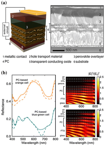
Figure 5. (a) Schematic of plasmonic effect in perovskite solar cells a: far-field scattering, b: near-field coupling, c: hot-electron transfer and d: plasmon resonant energy transfer. Reproduced with permission from Erwin et al., Energy Environ, Sci. 2016;9:1577. © 2016 Royal Society of Chemistry. (b) Optical absorbance of a mesoporous perovskite solar cell with and without popcorn-shaped Au –Ag nanoparticles, and corresponding EQE spectra. Reproduced with permission from Lu et al., RSC Advances. 2015;5:11175. © 2015 Royal Society of Chemistry. (c) Absorptance of the perovskite layer in Al2O3-based device without (control) and with Au@SiO2 NPs and corresponding incident photon-to-electron conversion efficiency (IPCE) spectra. Reproduced with permission from Zhang et al., Nano Lett. 2013;13:4505. © 2013 American Chemical Society.
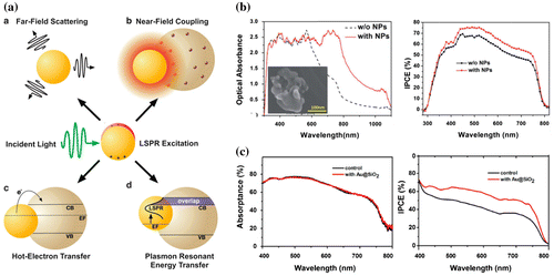
Table 2. Photovoltaic parameters of perovskite solar cells with the same fabrication parameters, with (‘NSs’) embedded plasmonic nanostructures, and without them (‘Ref’). The data have been taken from the corresponding references in the text.
Figure 6. (a) Cross-sectional scanning electron microscopy (SEM) image of perovskite solar cells with incorporated mesoporous (m-TiO2) and sub-micron TiO2 (s-TiO2) as scaffold layer. (b) finite-difference time-domain (FDTD) simulation model (I) and (II–IV) correspondingly simulated absorption profiles (at wavelength of 600 nm) for structured perovskite devices embedded with the m-TiO2, s-TiO2 and m&s-TiO2, respectively. Adapted with permission from Yin et al., RSC Advances 2016;6:24596. © 2016 Royal Society of Chemistry.
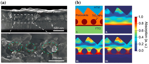
Figure 7. (a) Cross-sectional SEM of a perovskite solar cell fabricated on honeycomb structured SiO2 and (b) the J-V enhancement compared with that on planar substrate. Adapted with permission from Horantner et al., Energy Environ. Sci. 2015;8:2041. © 2015 Royal Society of Chemistry.
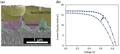
Figure 8. (a) Schematic illustration of the fabrication procedure: (I) A compact and (II) mesoporous TiO2 layer was subsequently deposited on the cleaned glass substrate, and (III) sintered to produce a dense/mesoporous bilayer film. (IV) A CH3NH3PbI3 precursor solution was spin-coated onto the substrate and a nitrogen gas stream was introduced to rapidly remove the solvent. (V) The film was finally annealed in an inert atmosphere, and (b) cross-sectional transmission electron microscopy (TEM) image of the textured perovskite. (c) IPCE spectrum (solid lines) of a planar perovskite device (grey line) and a textured perovskite device (black line). Adapted with permission from Pascoe et al., Adv. Funct. Mater. 2016;26:1278. © 2016 WILEY-VCH Verlag GmbH & Co. KGaA, Weinheim.
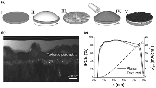
Figure 9. (a) Schematic illustration of nucleation and crystal growth in the formation of perovskite film with porous upper layer and (b) the cross-sectional SEM of the as formed film, (c) EQE enhancement of the device with porous upper layer (purple) compared with flat perovskite (orange). Adapted with permission from Yu et al., Nanoscale 2017;9:2569. © 2017 Royal Society of Chemistry.
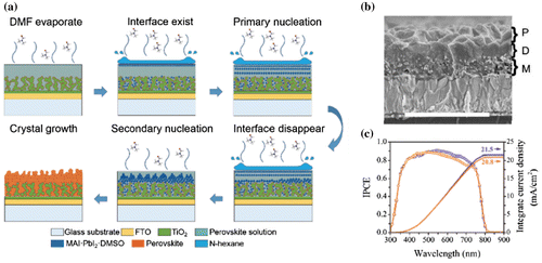
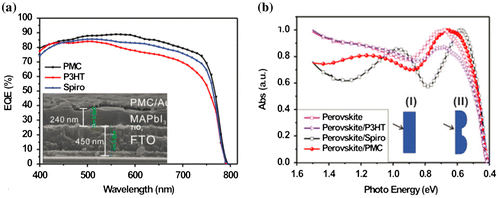
Figure 10. (a) EQE spectra of perovskite solar cells fabricated with different HTLs: P3HT, spiro-OMeTAD and spontaneously nanostructured P3HT/spiro-OMeTAD composite (‘PMC’). (b) Corresponding optical absorption spectra. Adapted with permission from Long et al., Nanoscale 2016;8:6290. © 2015 Royal Society of Chemistry.