Figures & data
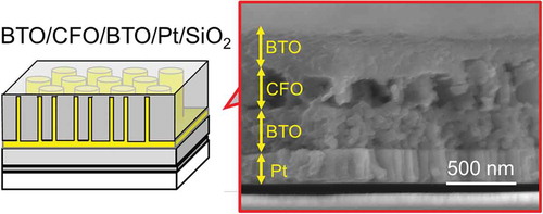
Figure 1. Schematic of the fabrication process for CFO nanotube arrays on a SiO2 substrate. The corresponding SEM images are shown to the right. From top to bottom: AAO template on a SiO2 substrate; CFO coated AAO on SiO2; CFO nanotube arrays on SiO2.
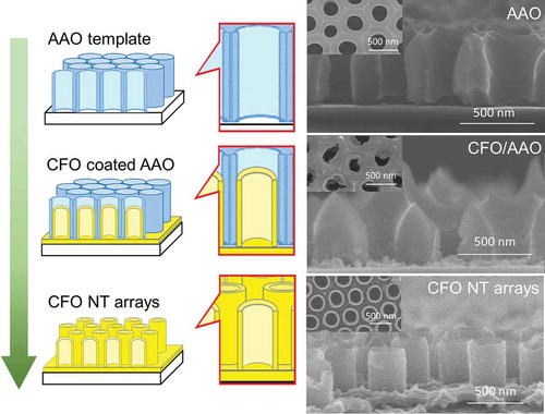
Figure 2. STEM (left) and the corresponding EDX images (right) of CFO coated AAO. In the EDX image, red and yellow colors represent Al and Co elements, respectively.
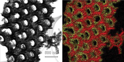
Figure 3. STEM (upper left), the corresponding EDX images (center and lower left) and SAED pattern (upper right) of CFO nanotubes. The XRD patterns of the CFO nanotube arrays on a SiO2 substrate and of CFO powder are shown at the lower right.
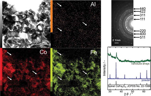
Figure 4. Schematic of the fabrication process for multiferroic nanocomposite, BTO/CFO/BTO, on a Pt-coated SiO2 substrate. The corresponding SEM images are shown to the right. From top to bottom: (AAO-placed) BTO compact layer on a Pt-coated SiO2 substrate; CFO nanotube arrays on BTO/Pt/SiO2; BTO coated CFO nanotube arrays on BTO/Pt/SiO2.
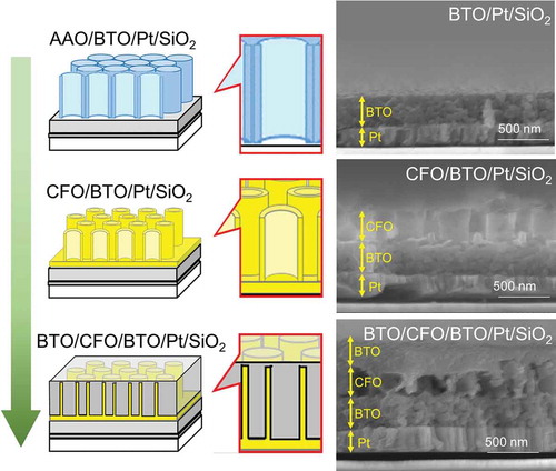
Figure 5. XRD pattern of the BTO compact layer on a Pt-coated SiO2 substrate.
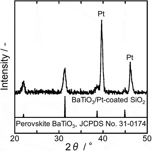
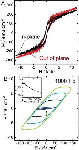
Figure 6. Magnetic (A) and dielectric (B) hysteresis loops of the multiferroic nanocomposite. The inset of the panel B shows the relative permittivity versus frequency.