Figures & data
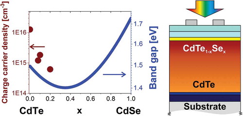
Figure 1. X-ray diffractograms of CdTe1-xSex thin films on glass substrate. The symbols indicate the CdTe reference from [Citation18] (PDF number 01–070–8041).
![Figure 1. X-ray diffractograms of CdTe1-xSex thin films on glass substrate. The symbols indicate the CdTe reference from [Citation18] (PDF number 01–070–8041).](/cms/asset/29179179-0457-4549-8a01-e6eedeac58d3/tsta_a_1497403_f0001_oc.jpg)
Figure 2. Splitting of the 311 Bragg reflex of CdTe1-xSex thin films on glass substrate. The reference value for the CdTe peak is from [Citation18].
![Figure 2. Splitting of the 311 Bragg reflex of CdTe1-xSex thin films on glass substrate. The reference value for the CdTe peak is from [Citation18].](/cms/asset/08863bd6-2f7e-4c61-9ae0-84eea704f0d6/tsta_a_1497403_f0002_oc.jpg)
Figure 3. Lattice constant of CdTe1-xSex thin films on glass substrate. The value for zinc blende CdSe (x = 1) was taken from literature [Citation23].
![Figure 3. Lattice constant of CdTe1-xSex thin films on glass substrate. The value for zinc blende CdSe (x = 1) was taken from literature [Citation23].](/cms/asset/48d8d4bf-0adf-4560-a357-729e67024695/tsta_a_1497403_f0003_oc.jpg)
Figure 4. Tauc plots of CdTe1-xSex thin films on glass substrate with linear fitting to extract the band gap.
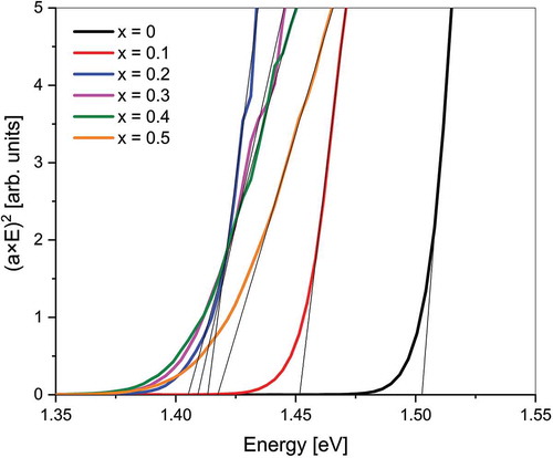
Figure 5. Band gap of CdTe1-xSex thin films on glass substrate determined from the Tauc plot. The band gap value for the pure CdSe (x = 1) was taken from literature [Citation25].
![Figure 5. Band gap of CdTe1-xSex thin films on glass substrate determined from the Tauc plot. The band gap value for the pure CdSe (x = 1) was taken from literature [Citation25].](/cms/asset/5b72180c-2dd7-41c1-a232-20bf356d58e0/tsta_a_1497403_f0005_oc.jpg)
Figure 6. Results from resistivity measurements with the transmission line method at 25 °C (a) and from Hall effect measurements at 70 °C (b–d) of CdTe1-xSex thin films on glass substrate with Cu doping variations for x = 0, 0.1, 0.2 and with an additional x = 0.08 sample with lower Cu doping.
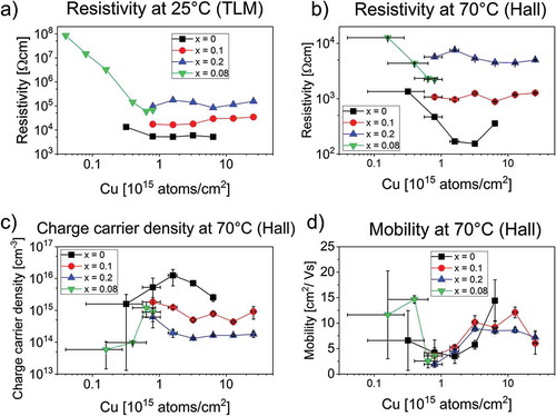
Table 1. Performance parameters of CdTe solar cells with and without CdTe1-xSex grading of the absorber towards the CdS window layer, and with varying CdS window layer thicknesses.
Figure 7. JV performance parameters of CdTe solar cells with and without CdTe1-xSex grading of the absorber towards the CdS window layer, and with varying CdS window layer thicknesses.
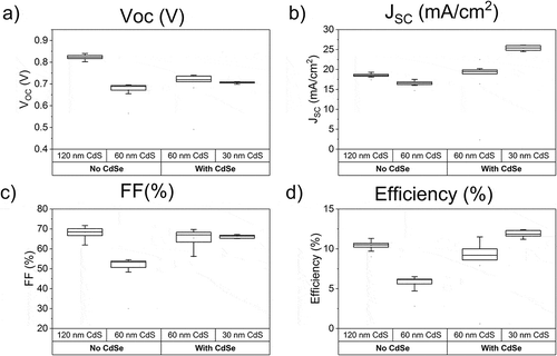
Figure 8. Current-voltage curves of CdTe solar cells with and without CdTe1-xSex grading of the absorber towards the CdS window layer, and with varying CdS window layer thicknesses.
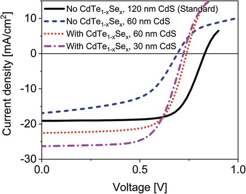
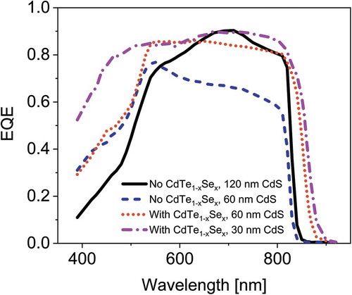
Figure 9. External quantum efficiency of CdTe solar cells with and without CdTe1-xSex grading of the absorber towards the CdS window layer, and with varying CdS window layer thicknesses.