Figures & data
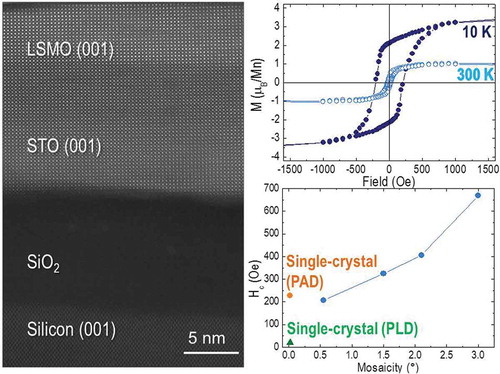
Figure 1. Top. Schematic diagram showing the novel synthetic route combining MBE and PAD to obtain epitaxial (001) LSMO thin films on (001) STO/Si buffer layers. Bottom. Left: RHEED image along the [100] and [110] azimuths of the STO film grown by MBE. Right: RHEED image along the [100] and [110] azimuths of the LSMO film deposited by PAD on STO/Si at 950 °C during 2 h.
![Figure 1. Top. Schematic diagram showing the novel synthetic route combining MBE and PAD to obtain epitaxial (001) LSMO thin films on (001) STO/Si buffer layers. Bottom. Left: RHEED image along the [100] and [110] azimuths of the STO film grown by MBE. Right: RHEED image along the [100] and [110] azimuths of the LSMO film deposited by PAD on STO/Si at 950 °C during 2 h.](/cms/asset/63dae268-2ec5-47a2-8614-c043c41acc96/tsta_a_1520590_f0001_oc.jpg)
Figure 2. Atomic resolution Z-contrast image of LSMOPAD/STOMBE/Si heterostructure viewed along the [100]-crystallographic direction. Detail of the Z-contrast image showing the coherent interface between the LSMO and the STO/Si buffer layers (left image). EELS image (right): color elemental mapping produced by overlaying the Mn L2,3 (green), Ti L2,3 (blue), Sr M4,5 (red), and La M4,5 (orange) elemental maps, displaying a high-quality chemical interface between STO and LSMO layer, the structure of which is sketched in the left of the image, respectively.
![Figure 2. Atomic resolution Z-contrast image of LSMOPAD/STOMBE/Si heterostructure viewed along the [100]-crystallographic direction. Detail of the Z-contrast image showing the coherent interface between the LSMO and the STO/Si buffer layers (left image). EELS image (right): color elemental mapping produced by overlaying the Mn L2,3 (green), Ti L2,3 (blue), Sr M4,5 (red), and La M4,5 (orange) elemental maps, displaying a high-quality chemical interface between STO and LSMO layer, the structure of which is sketched in the left of the image, respectively.](/cms/asset/24992639-d5a8-4777-85b3-a5274985f5f7/tsta_a_1520590_f0002_oc.jpg)
Figure 3. a) XRD pattern of the LSMOPAD/STOMBE/Si film in a θ-2θ configuration. b) XRD pattern around the (002) Bragg reflection of the perovskite with 2.5 times more time per step. c) Pole figure with a 45° tilt of χ (Chi) containing both (202) reflections for LSMO/STO and silicon. d) Real space representation from reciprocal space mapping (RSM) around the (−204) Bragg peak of the perovskite containing both the STOMBE as the LSMOPAD layers.
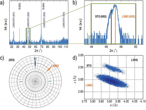
Figure 4. a) Temperature dependence of the resistivity measured in N2 up to 400 K in a Van der Pauw configuration for LSMO films deposited on top of non-annealed (cyan) and annealed (blue) STO-buffered Si substrates. b) Field-cooled temperature dependence of the magnetization (Bohr magneton per atom of manganese) in an applied in-plane magnetic field of 1000 Oe for the LSMOPAD/STOMBE/Si film. c) In-plane field dependence (Bohr magneton per atom of manganese at 10 K and 300 K) of the magnetization. d) Magnetoresistance at 300 K. Data corresponds to LSMO films deposited on STO/Si substrate with a mosaicity value of 1°.
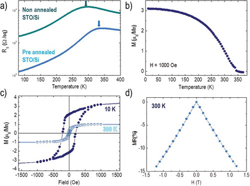
Figure 5. a) FWHM values, obtained from rocking curves of the (002) peak of STO for STO/Si buffer layers with different mosaicity degrees. b) Atomic resolution Z-contrast image viewed along the [100]-crystallographic direction to compare two STO/Si samples with 0.6° (bottom) and 3.0° (up) FWHM values.
![Figure 5. a) FWHM values, obtained from rocking curves of the (002) peak of STO for STO/Si buffer layers with different mosaicity degrees. b) Atomic resolution Z-contrast image viewed along the [100]-crystallographic direction to compare two STO/Si samples with 0.6° (bottom) and 3.0° (up) FWHM values.](/cms/asset/78b04154-fa7f-4cd2-bcd6-bc4469409994/tsta_a_1520590_f0005_oc.jpg)
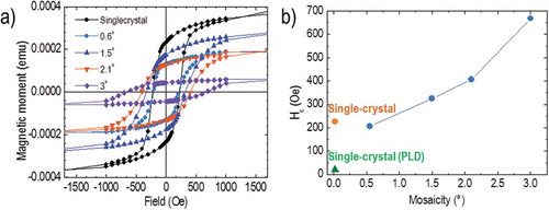
Figure 6. a) Hysteresis loops at 10 K for LSMO/STO/Si films as a function of the mosaicity from single-crystal up to FWHM of 3°. b) Evolution of the LSMO coercivity as a function of mosaicity of the STO-buffered silicon substrates.