Figures & data
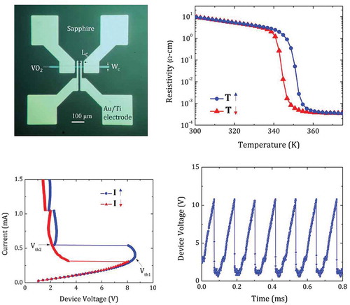
Figure 1. Optical microscope image of a D20 VO2 micro-channel device. (b) The change in VO2 resistivity for increasing and decreasing temperatures.
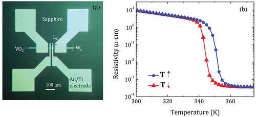
Figure 2. I–V curves for devices D10 (a) and D20 (b) under VC mode of operation at increasing (•) or decreasing (▲) device voltage. The insets show the corresponding I–V curves at increasing or decreasing total voltage in the circuit. Measurements were performed with fixed Rext = 4.0 kΩ and TS = 64 °C for both devices. Points Vth1 and Vth2 are the threshold voltages corresponding to the forward and the reverse IMT, respectively.
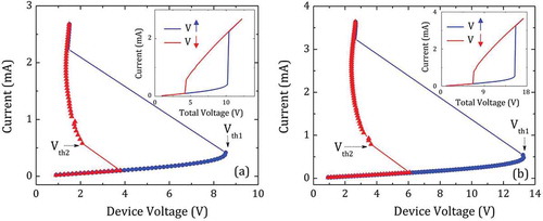
Figure 3. I-V curves for devices D10 (a) and D20 (b) under CC mode of operation at increasing (•) or decreasing (▲) device current. Measurements were performed with fixed Rext = 4.0 kΩ and TS = 64 °C. Points Vth1 and Vth2 are the threshold voltages corresponding to the forward and the reverse IMT, respectively.
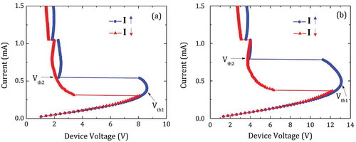
Figure 4. Electrical oscillation waveforms obtained under CC mode of operation for devices D10 (a) and D20 (b). Measurements were obtained at fixed ISP = 0.8 mA, Rext = 1.5 kΩ and TS = 64 °C.
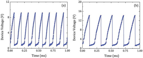
Figure 5. Electrical oscillation waveform obtained under CC mode of operation for a D10 device without any external series resistance. The measurement was carried out at fixed ISP = 0.6 mA and TS = 60 °C.
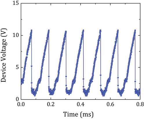
Figure 6. Electrical oscillation waveforms obtained under CC mode of operation for a D10 device at fixed ISP = 1 mA, Rext = 1.5 kΩ and TS = 60 °C. (a) no laser illumination and (b) illuminated by a laser with Po ≈ 455 W/cm2. (c) Measured oscillation frequencies and (d) peak-to-peak amplitude voltage for a D10 device at different laser power densities. The dashed straight lines in (c) and (d) are guides to the eye.
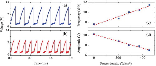
Figure 7. Nonlinear square fittings of the exponential part of the voltage build-up in the VO2 micro-channel for one oscillation cycle for: (a) device D10: ISP = 1 mA and ISP = 0.6 mA with fixed TS = 60 °C and Rext = 1.5 kΩ. The inset shows the schematic of the physical equivalent circuit for the VO2 micro-channel devices. (b) Device D10: Rext = 0 Ω and Rext = 1.5 kΩ with fixed ISP = 0.6 mA and TS = 60 °C.
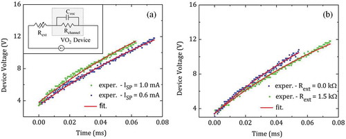
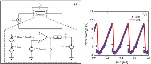
Figure 8. (a) Equivalent circuit model for the VO2 micro-channel devices. (b) Simulated and experimental waveforms for a D10 device with ISP = 0.6 mA, Rext = 0 Ω, and Ts = 60 °C.