Figures & data
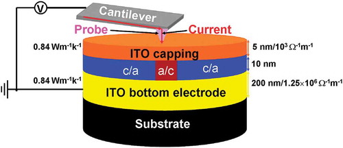
Figure 1. Electrical probe memory operated in (a) write mode and (c) readout mode, and the corresponding physical principle for (b) write process and (d) readout process.
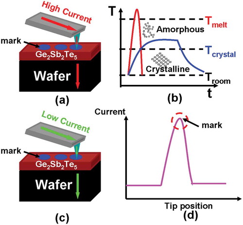
Figure 2. (a) The electrical (σ) and thermal (k) conductivity values of ITO films for different thickness and (b) several predefined points where phase-transformation temperature is calculated.
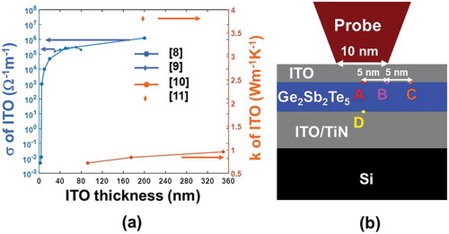
Figure 3. Comparison between an experimental I–V curve from a typical cell consisting of a 7-nm amorphous Ge2Sb2Te5 layer sandwiched by a 10-nm ITO top layer and a 50-nm ITO bottom layer and that calculated based on our theoretical model. The experimental I–V curve is replotted from Ref. [Citation18].
![Figure 3. Comparison between an experimental I–V curve from a typical cell consisting of a 7-nm amorphous Ge2Sb2Te5 layer sandwiched by a 10-nm ITO top layer and a 50-nm ITO bottom layer and that calculated based on our theoretical model. The experimental I–V curve is replotted from Ref. [Citation18].](/cms/asset/94e7b404-25c9-4d0b-b5b9-77ccf6db732b/tsta_a_1534072_f0003_oc.jpg)
Table 1. Characteristic parameters used in simulations.
Figure 4. Temperature contours at points A, B, C, D as a function of electrical conductivity (σ) and thickness of the ITO capping layer during (a) crystallization and (b) amorphization processes. For both simulations, the thermal conductivity of the capping layer remains at 0.84 W m−1 K−1, while the bottom layer is assumed to be TiN layer with a thickness, an electrical conductivity, and a thermal conductivity of 40 nm, 106 Ω−1 m−1, and 12 W m−1 K−1, respectively. Note that for (a) maximum temperature contours of 1400 °C at A and 400 °C at C are outside this figure and, therefore, are not visible. The red arrow indicates the direction along which the temperature increases.
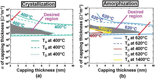
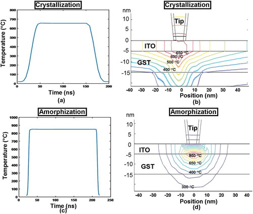
Figure 5. The temperature variation in the middle of the ITO capping (directly underneath the tip) as a function of the pulse time for (a) crystallization and (b) amorphization, and the electric field distribution inside the ITO capping at the onset of the pulse plateau for (c) crystallization and (d) amorphization. The electrical conductivity, thickness, and thermal conductivity of the capping layer are set to be 103 Ω−1 m−1, 5 nm, and 0.84 W m−1 K−1, while other parameters are as for .
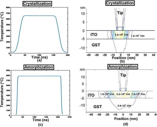
Figure 6. Temperature contours at points A, B, C, D as a function of thermal conductivity (k) and thickness of the ITO capping layer during (a) crystallization and (b) amorphization processes. For both simulations, the thickness and the electrical conductivity of the capping layer remain at 5 nm and 103 Ω−1 m−1, while other parameters are as for . Note that for both figures, maximum temperature contours of 1400 °C at A and 400 °C at C are outside the range and, therefore, are not visible. The red arrow indicates the direction along which the temperature increases.
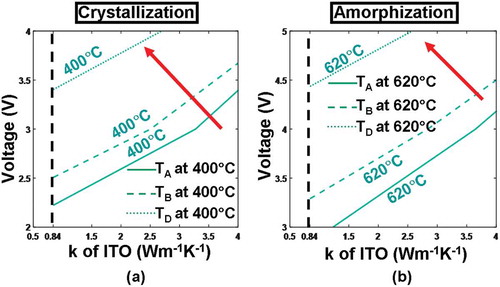
Figure 7. Temperature contours at points A, B, C, D as a function of electrical conductivity (σ) and thickness of the ITO bottom layer during (a) crystallization and (b) amorphization processes. For both simulations, the thickness, the electrical conductivity, and the thermal conductivity of the capping layer remain at 5 nm, 103 Ω−1 m−1, and 0.84 Wm−1 K−1, while the thermal conductivity of the ITO bottom layer remains at 0.84 Wm−1 K−1. Note that for (a) maximum temperature contours of 1400 °C at A and 400 °C at C are outside the range and, therefore, are not visible. The red arrow indicates the direction along which the temperature increases.
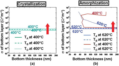
Figure 8. Temperature contours at points A, B, C, D as a function of thermal conductivity (k) and thickness of the ITO bottom layer during (a) crystallization and (b) amorphization processes. For both simulations, the thickness, the electrical conductivity, and the thermal conductivity of the capping layer remain at 5 nm, 103 Ω−1 m−1, 0.84 W m−1 K−1, while other parameters are as for . Note that for both figures, maximum temperature contours of 1400 °C at A and 400 °C at C are outside the range and, therefore, are not visible. The red arrow indicates the direction along which the temperature of these points increases.
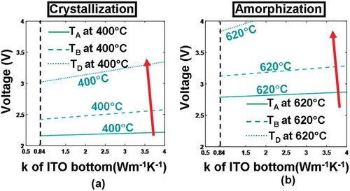
Figure 9. Schematic of the optimized electrical probe memory with ITO capping and bottom layers. ‘c’ and ‘a’ represent crystalline and amorphous phases, respectively.

Figure 10. The resultant bit array in (a) crystalline and (b) amorphous phase from the optimized probe device with ITO capping and bottom layers. The insets show the cross-sectional view of the formed bits.
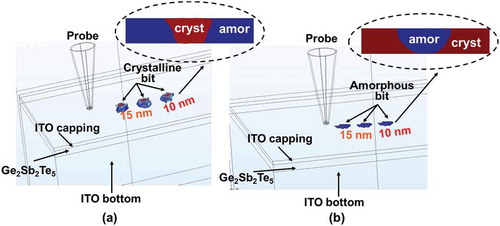
Figure 11. Temperature variation at point A as a function of the pulse time for (a) crystallization and (c) amorphization, and the temperature distribution at point A at the onset of the pulse plateau for (d) crystallization and (d) amorphization. The modeling parameters are as for .