
Figures & data
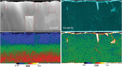
Figure 1. Selected sections of XRD patterns of Samples 1 (growth interrupted before the 1st stoichiometry point) and 2 (growth interrupted just after the 1st stoichiometry point) with corresponding cross-sectional SEM micrographs.
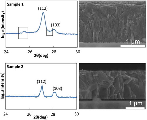
Figure 2. Sample 1: STEM-HAADF (top left), EDX Cu at.% map (top-right), GGI map (bottom-left) and CGI map (bottom-right).
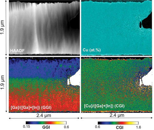
Figure 3. Sample 2: STEM-HAADF (top left), EDX Cu at.% map (top-right), GGI map (bottom-left), and CGI map (bottom-right).
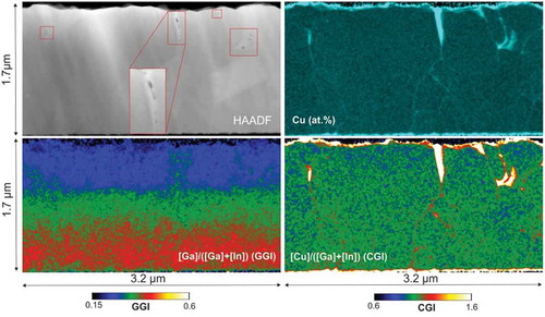
Figure 4. Sample 3: STEM-HAADF (top left), EDX Cu at.% map (top-right), GGI map (bottom-left), and CGI map (bottom-right).
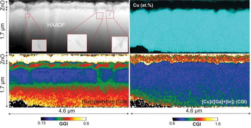
Figure 5. Sample 3. Top: HAADF-STEM micrograph of a completed CIGS solar cell and BF image of a selection of the same area (selection of BF image of the area at the right-hand side of the HAADF-STEM micrograph is shown for a better view). A large density of voids with diameters of up to 50 nm can be observed below the surface. Bottom: EDX spectra of selected areas.
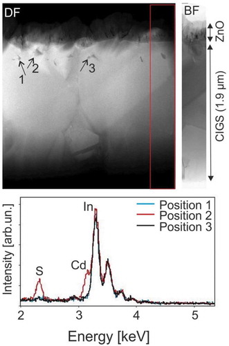
Figure 6. SEM micrograph of a completed CIGS sample surface (equivalent to Sample 3) after sputtering with Ga FIB on a 10 x 10 μm2 area (20 keV, 182 pA).
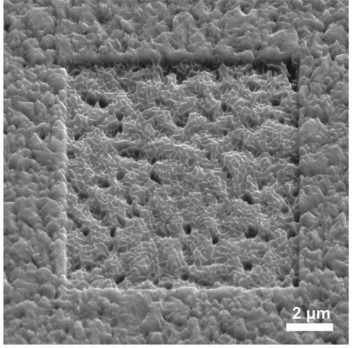
Figure 7. Sample 3: Left: STEM/EDX GGI map. Top-right: GGI grading as measured by SIMS depth profiling. Bottom-right: GGI gradings from the STEM/EDX GGI map along cross-sectional lines with 20 nm thickness (the value at each point is the average over the given thickness). Thickness scaling of SIMS depth profile is made according to the one measured by STEM for comparison.
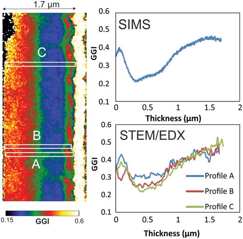
Figure 8. GGI gradings used for Sentaurus 2D simulations. ‘High-GGI’ profile and ‘low-GGI’ profile have been employed in a inhomogeneous 2-section structure with a 15%–85% width ratios, respectively. The baseline grading corresponds to the average composition at each depth, weighted over the respective width. The baseline grading profile was also used to simulate the performance of a reference homogeneous structure.
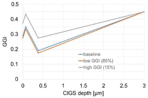
Figure 9. Structures employed in three-dimensional void simulations. Three-dimensionality is obtained by rotation around the edge at the right-hand side of each structure, creating cylindrical shapes for both the solar cell stacks and the voids. Right: the void is adjacent to the CdS buffer layer. Left: the void is buried 50 nm beneath the CIGS surface.
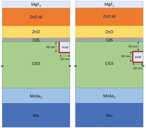
Table 1. Simulated J-V parameters of different cylindrical structure with and without voids, depending on surface recombination velocities.