
Figures & data
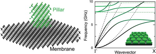
Figure 1. Phonon dispersion of a pillar-based PnC (solid lines), a silicon membrane (dashed lines), and resonant frequencies of a pillar (horizontal dash-dotted lines). The color of the branches shows the physical location of the modes (ξ). Details of the simulated structure can be found in Ref [Citation30].
![Figure 1. Phonon dispersion of a pillar-based PnC (solid lines), a silicon membrane (dashed lines), and resonant frequencies of a pillar (horizontal dash-dotted lines). The color of the branches shows the physical location of the modes (ξ). Details of the simulated structure can be found in Ref [Citation30].](/cms/asset/5ce73ef0-2cbe-486f-91ed-38b87ff4c241/tsta_a_1542524_f0001_oc.jpg)
Figure 2. (a) Schematic of the sample used by Achaoui et al. [Citation36] to study the phonon transmission through an array of nickel pillars of 6.4 µm in diameter and 4.7 µm in height. (b) Transmittance spectrum shows a phononic bandgap. (c) The out-of-plane displacement map shows the reflection of 170 MHz phonons from the PnC region. Reprinted figure with permission from [Citation36]. Copyright 2018 by the American physical Society.
![Figure 2. (a) Schematic of the sample used by Achaoui et al. [Citation36] to study the phonon transmission through an array of nickel pillars of 6.4 µm in diameter and 4.7 µm in height. (b) Transmittance spectrum shows a phononic bandgap. (c) The out-of-plane displacement map shows the reflection of 170 MHz phonons from the PnC region. Reprinted figure with permission from [Citation36]. Copyright 2018 by the American physical Society.](/cms/asset/359ba2f1-6c79-4882-ad00-df5aa75bc3e8/tsta_a_1542524_f0002_oc.jpg)
Figure 3. (a) Lithium niobate pillar-based PnC with pillars of 240 nm in diameter and 225 nm in height [Citation49]. (b) Phonon dispersion of a PnC measured using Brillouin light scattering technique. The experimental data (black dots) agree with the result of the FEM simulations (small blue dots). Reprinted figure with permission from [Citation49]. Copyright 2018 by the American Physical Society.
![Figure 3. (a) Lithium niobate pillar-based PnC with pillars of 240 nm in diameter and 225 nm in height [Citation49]. (b) Phonon dispersion of a PnC measured using Brillouin light scattering technique. The experimental data (black dots) agree with the result of the FEM simulations (small blue dots). Reprinted figure with permission from [Citation49]. Copyright 2018 by the American Physical Society.](/cms/asset/f1611c1b-6cf9-4db2-b3ea-431b20883293/tsta_a_1542524_f0003_oc.jpg)
Figure 4. Example of a molecular dynamics model of a pillar-based PnC and the dependence of the thermal conductivity normalized by that of a membrane on the pillar height (t) found in Refs [Citation33,Citation34,Citation55,Citation58].
![Figure 4. Example of a molecular dynamics model of a pillar-based PnC and the dependence of the thermal conductivity normalized by that of a membrane on the pillar height (t) found in Refs [Citation33,Citation34,Citation55,Citation58].](/cms/asset/3bfdd56c-5c15-4971-93b1-bbd7dae7139f/tsta_a_1542524_f0004_oc.jpg)
Figure 5. (a) Relative heat capacity of bulk silicon samples with pillars on the surface measured by Iskandar et al. [Citation62] at room temperature. The inset shows one of the samples (the shape and size are different for every sample). Reprinted from [Citation62], with the permission of AIP Publishing. (b) The thermal conductivity of the nanobeams with pillars of different diameters measured by Anufriev et al. [Citation63] at room temperature. The inset shows the fragment of the nanobeam and transmission electron microscopy image of the pillar/beam interface featuring surface roughness.
![Figure 5. (a) Relative heat capacity of bulk silicon samples with pillars on the surface measured by Iskandar et al. [Citation62] at room temperature. The inset shows one of the samples (the shape and size are different for every sample). Reprinted from [Citation62], with the permission of AIP Publishing. (b) The thermal conductivity of the nanobeams with pillars of different diameters measured by Anufriev et al. [Citation63] at room temperature. The inset shows the fragment of the nanobeam and transmission electron microscopy image of the pillar/beam interface featuring surface roughness.](/cms/asset/f1004154-f90e-4312-ab93-401616667b8d/tsta_a_1542524_f0005_oc.jpg)