Figures & data

Figure 1. (a) Schematic diagram of isolated Fe3O4/GeOx/Ge NC memory (left image). The formation of high-crystallinity Fe3O4 and high-purity GeOx at the interface between Fe3O4 and Ge (right image) aiming at high resistive switching performance. (b) Resistive switching mechanism in Fe3O4/GeOx/Ge NCs that have some unclearness: high resistance layer (HRL) which is a key for nanoionics-based resistive switching
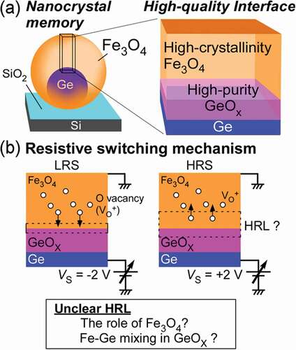
Figure 2. (a) AFM image, (b) RHEED pattern, and (c) The IS-VS curve of as-grown NCs with the Fe coating layer of 30 MLs. The VS was swept in the following order: (1) 0V→ 2V, (2) 2V → 0V, (3) 0V → −2V, and (4) −2V → 0V. (d) FWHM of 224Fe3O4 (left axis) and Pswitch (right axis) as a function of the deposition amount of Fe coating layer in as-grown NCs (the solid squares and circles, respectively). The open square and circle denote the FWHM of 224Fe3O4 and Pswitch in NCs annealed at 250°C, respectively. (e) Schematic of the Fe3O4 crystallinity effect on the resistive switching characteristics, where low- and high-crystallinity Fe3O4 are denoted as LC-Fe3O4 and HC-Fe3O4. Electric-field-applied region gets smaller in Fe3O4 with more oxygen vacancies (VO+) because of large screening effect by high concentration carriers
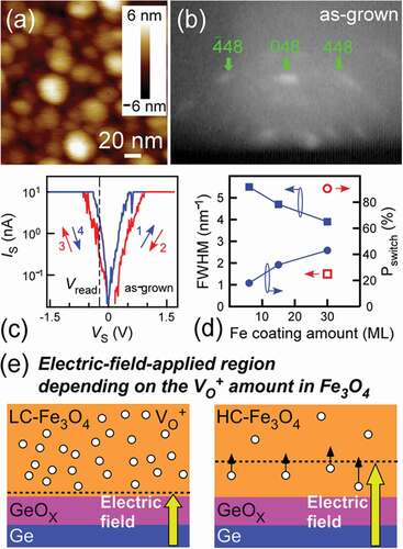
Figure 3. (a) FWHM estimated from 224Fe3O4 peak in RHEED (left axis) and Fe-Ge mixing ratio measured from XPS spectra (right axis) in each sample (as-grown: as-grown NCs, 250: NCs annealed at 250°C, and 400: NCs annealed at 400°C). (b) Low-magnification HRTEM image of NCs annealed at 250°C. (c) Enlarged HRTEM image of the square region in (b). FFT patterns of (d) regions B and (e) A in (c). The region marked by the broken line denotes GeOx. Theoretical FFT patterns of (f) Fe3O4 and (g) Ge
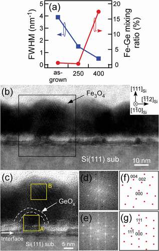
Figure 4. The IS-VS curves of (a) NCs annealed at 250°C and (b) at 400°C. (c) Pswitch and Off/On ratio of all the NCs. The solid squares and circles denote the Pswitch and the Off/On ratio, respectively. (d) Schematic of the GeOx quality effect on the resistive switching characteristics
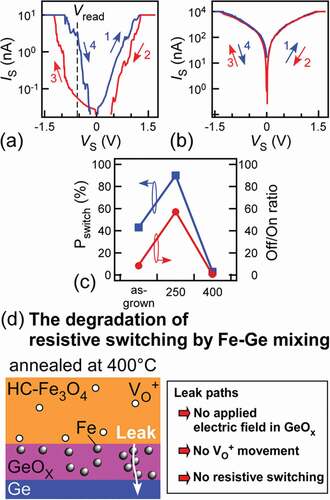
Figure 5. Resistive switching mechanism in Fe3O4/GeOx/Ge NCs
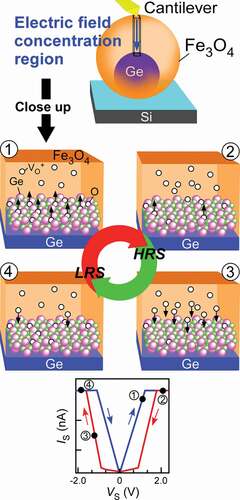
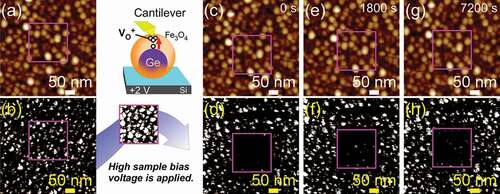
Figure 6. Memory effect of NCs annealed at 250°C (a, c, e, g) AFM and (b, d, f, h) current mapping images of the NCs at the VS of −0.5V: (a, b) before applying VS of +2V, (c, d) just after applying VS of +2V, (e, f) 1800 s later since the resistive switching, and (g, h) 7200 s later since the resistive switching, respectively. The current mapping image when applying VS of +2V is shown in the inset