
Figures & data

Table 1. Summary of the samples produced and their thicknesses
Figure 1. (a) SEM micrograph and (b) and (c) AFM images of the surface of the sputtered film with 46 nm thickness. (d) SEM micrograph and (e) and (f) AFM images of the surface of the sputtered film with 500 nm thickness
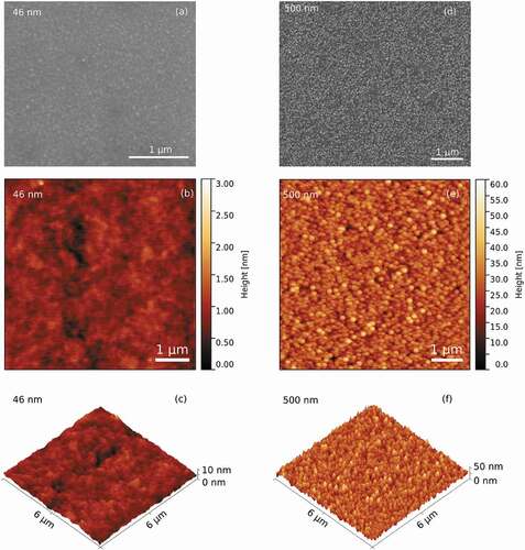
Figure 2. Evolution of the roughness for the sputtered and electrodeposited films as a function of the film’s thickness
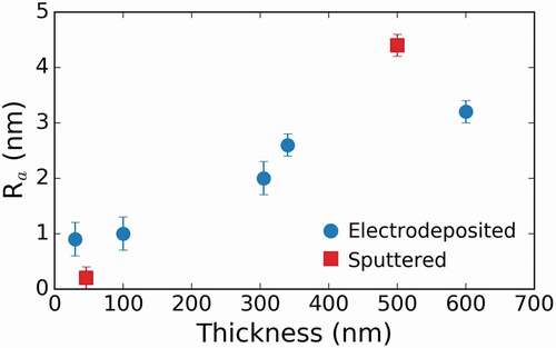
Figure 3. GIXRD plots labeled by film thickness from: (a) sputtered and (b) electrodeposited films. Intensity values are reported in linear scale. Unlabeled peaks in (a) belong to the substrate. Inset of panel (b) shows the geometry of the GIXRD set-up used for the acquisition of the GIXRD plots
Table 2. Values for the angular position (2 %\θ%), full width at half maximum (FWHM) and average crystal size < D > for the sputtered films, the latter calculated by applying the Scherrer’s formula on (110) peak width of the α -(Fe,Pd) phase
Figure 4. (a) SEM micrograph and (b) and (c) AFM images of the surface of the electrodeposited film with 30 nm thickness. (d) SEM micrograph and (e) and (f) AFM images of the surface of the electrodeposited film with 600 nm thickness
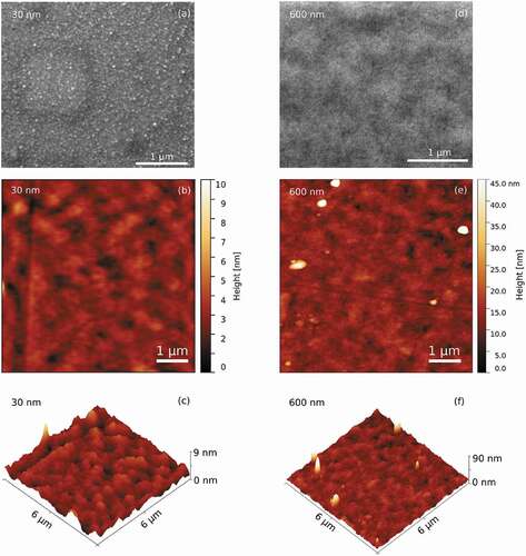
Figure 5. TEM images of the cross-section of the (a) 30 nm and (b) 600 nm thick electrodeposited films
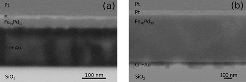
Table 3. Values for the angular position, full width at half maximum (FWHM) and average crystal size < D > for the electrodeposited films, the latter calculated by applying the Scherrer’s formula on the (110) peak width of the α -(Fe,Pd) phase
Figure 6. Hysteresis loops, measured at room temperature, for the in-plane orientation of the field corresponding to the (a) sputtered and (b) electrodeposited films with varying thickness. The insets show the evolution of the coercive field as a function of the film thickness for the sputtered and electrodeposited films
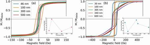
Figure 7. Room temperature MFM images, acquired at magnetic remanence, for the electrodeposited films with a thickness of (a) 600 nm, (b) 340 nm, (c) 305 nm and (d) 30 nm
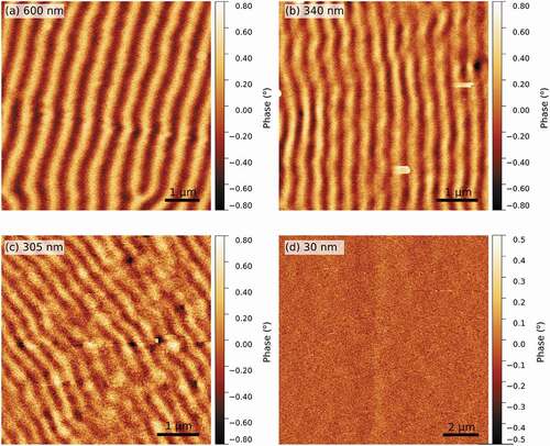
Figure 8. Load-displacement nanoindentation curves of the: (a) 305 nm thick electrodeposited (circles) and 300 nm thick sputtered (squares) films and (b) 600 nm thick electrodeposited (circles) and 500 nm thick sputtered (squares) films
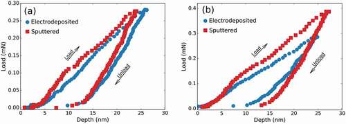
Table 4. Berkovich nanohardness (HB), reduced Young’s modulus (Er), HB/Er, H/E
and Ue/Utot for sputtered Fe70Pd30 films of varying thickness (t)
Table 5. Berkovich nanohardness (HB), reduced Young’s modulus (Er), HB/Er, H/E
and Ue/Utot for electrodeposited Fe70Pd30 films of varying thickness (t)