Figures & data
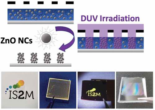
Figure 1. Schematic of DUV photopatterning showing the role of 2-ethylhexanoate ligand in the photolithography process.
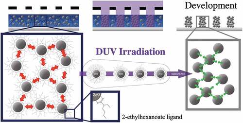
Figure 2. (a) Photographs of the colloidal solution of ZnO NCs capped with 2-ethylhexanoate ligands, under visible (left) and 365 nm UV illumination (right). (b) HRTEM images of the ZnO NCs functionalized with 2-ethylhexanoate ligands. (c) Particle size distribution of the ZnO NCs functionalized with 2-ethylhexanoate ligands.
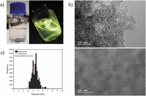
Figure 3. Relation between the zinc-based surface modifier precursors used to prepare the ZnO NCs, the stability of the colloids in solution and the solubility of the obtained thin films by spin-coating.
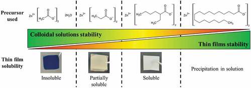
Figure 4. (a) FTIR spectra of ZnO NCs thin film prepared from ZnO:2-ethylhexanoate precursor and their evolution under DUV irradiation. (b) FTIR spectra of ZnO NCs thin film prepared from Zn:2-ethylhexanoate precursor at different ageing time at ambient atmosphere. (c) Evolution of thickness (evaluated by spectroscopic ellipsometry) under DUV and thermal annealing. (d) AFM images of the surface after DUV annealing (10 J.cm−2).
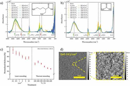
Figure 5. XPS analysis of the material prepared by spin-coating, DUV and thermal annealing. (a) C and O molar ratio (versus Zn) extracted from XPS data (details of data are shown in Table S1 and S2). (b) Analysis of C1s peak. (c) Analysis of O1s peak.
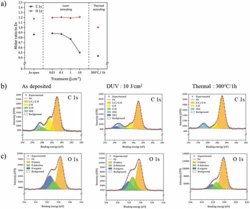
Figure 6. Grazing incidence X-ray diffraction analysis of the ZnO NCs thin films with (a) DUV treatment and (b) thermal treatment. (c) Crystallite size calculated from XRD data using the Scherrer equation for as-spin film (AS) and films after DUV and thermal annealing.
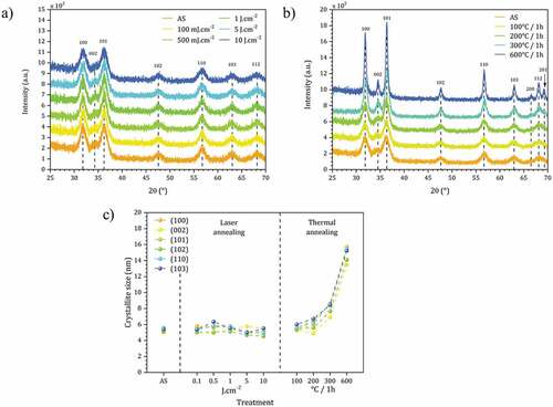
Figure 7. (a) Tauc plots of ZnO NCs thin film (as deposited (AS), with DUV treatment and thermal annealing). (b) Emission spectra of ZnO NCs thin films with different curing conditions under 350 nm excitation. (c) Excitation-emission maps of ZnO NCs thin films with different curing conditions and associated visible luminescence images of the thin film under 365 nm excitation.
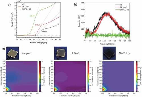
Figure 8. Topography AFM images of photostructured films with a binary mask of 1.6 µm period (line/space ratio :1/1) for doses between 200 and 600 mJ.cm-2. Films of 80 nm initial thicknesses are irradiated directly after spin-coating and developed in cyclohexanone for 60 s. Bottom: cross section along x direction for the above four AFM images.
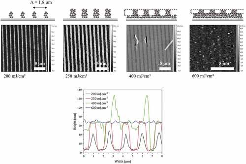
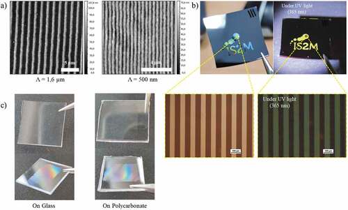
Figure 9. (a) AFM images of 10 µm and 500 nm period microstructures on silicon. (b) Photographs of a sample prepared with a mask showing the laboratory logo under visible and UV illumination and microscopy images under visible and UV illumination (scale bar 100 µm). (c) Examples of ZnO NC arrays prepared on glass and polycarbonate substrates.