Figures & data
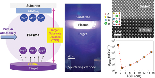
Figure 1. (a) A schematic illustration of the sputtering process employed in a sputtering chamber for deposition of SrMoO3 thin films from a SrMoO4 sintered target; (b) a photograph of the sputtering chamber during deposition with TSD of 2.5 cm.
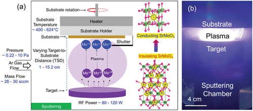
Figure 2. RHEED patterns for the surface of SMO (30 nm) films deposited at Ts = 624°C on STO(001) substrates with the incident electron beam parallel to (a)-(c) STO[100] and (d)-(f) STO[110] azimuth, respectively. (a) and (d) TSD = 1.0 cm, (b) and (e) 2.5 cm, and (c) and (f) 6.2 cm, respectively.
![Figure 2. RHEED patterns for the surface of SMO (30 nm) films deposited at Ts = 624°C on STO(001) substrates with the incident electron beam parallel to (a)-(c) STO[100] and (d)-(f) STO[110] azimuth, respectively. (a) and (d) TSD = 1.0 cm, (b) and (e) 2.5 cm, and (c) and (f) 6.2 cm, respectively.](/cms/asset/5d6339d9-6521-41f3-bd92-e4a178c13b1e/tsta_a_2378684_f0002_oc.jpg)
Figure 3. TSD dependence of P-V and Ra for SMO (30 nm) films. The inset shows AFM images for TSD = 1.0 cm and TSD = 2.5 cm.
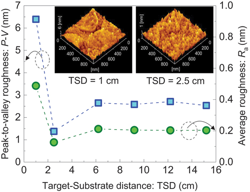
Figure 4. (a) Out-of-plane XRD patterns for various TSDs of SMO (30 nm) films. (b) RSM results around the STO(204) and SMO(204) reflections and (c) ϕ-scan pattern of the SMO(204) lattice planes for TSD = 2.5 cm and Ts = 624°C.
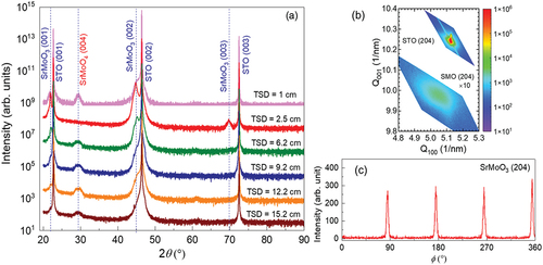
Figure 5. (a) Low magnification cross-sectional HAADF-STEM image of SMO film on STO(001) substrate. (b) and (c) are [001] NBED patterns acquired along SMO[100] and STO[100], respectively. (d) EDS maps collected from the region marked by a dashed-line rectangular frame in (a), and (e) corresponding EDS line profiles. (f) High magnification HAADF-STEM image near the SMO(001)/STO(001) interface. (g) IFFT filtered outline image of (f). The inset of (g) shows the FFT image of (f) and filter areas (dotted circles) for obtaining (g).
![Figure 5. (a) Low magnification cross-sectional HAADF-STEM image of SMO film on STO(001) substrate. (b) and (c) are [001] NBED patterns acquired along SMO[100] and STO[100], respectively. (d) EDS maps collected from the region marked by a dashed-line rectangular frame in (a), and (e) corresponding EDS line profiles. (f) High magnification HAADF-STEM image near the SMO(001)/STO(001) interface. (g) IFFT filtered outline image of (f). The inset of (g) shows the FFT image of (f) and filter areas (dotted circles) for obtaining (g).](/cms/asset/cca20d2d-9ef6-4a4f-a4af-64bc46760fb2/tsta_a_2378684_f0005_oc.jpg)
Figure 6. (a) TSD dependence of the resistivity at 300 K (ρ300K) of the SMO films, (b) ρ300K as a function of the SMO thickness for TSD = 2.5 cm. (c) temperature dependence of the resistivity: upper panel: TSD = 1.0 cm, lower panel: 2.5 cm, 6.2 cm and 15.2 cm. The green solid line of the upper panel indicates the fitting result of Equation (2). The red solid lines of the lower panel indicate fitting results using Equation (1).
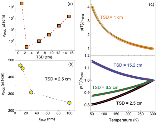
Table 1. The fitting parameters , A, and B obtained from fitting in using Equation (1).
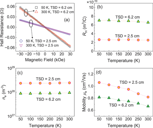
Figure 7. (a) Out-of-plane magnetic field dependence of hall resistance at 50 and 300 K of the films for TSD = 2.5 and 6.2 cm. Temperature-dependences of (b) RH, (c) ne, and (d) μe.