
Figures & data
Table 1. Main characteristics of the studied microwires.
Figure 1. SEM image of a portion of the characterised as-cast microwire and contour plot of GND density over a length of 500
.
![Figure 1. SEM image of a portion of the characterised as-cast microwire and contour plot of GND density logρGND[m−2] over a length of 500 μm.](/cms/asset/81b0cc6e-c65d-4243-8e48-db8e92df07e4/tphm_a_1605220_f0001_oc.jpg)
Figure 2. (a) SEM image and contour plots of (b) misorientation angle [] and (c) dislocation density
in single-slip oriented microwire SS1. (d) Intensity distribution of 6 diffraction peaks at two locations (indicated by labels 1 and 2 on the above maps) and theoretical streaking directions for the glide systems a3, c5 and b2 (Schmid factors before/after deformation of respectively
0.46/0.41, 0.11/0.41 and 0.34/0); window size :
pixels.
![Figure 2. (a) SEM image and contour plots of (b) misorientation angle [∘] and (c) dislocation density logρGND[m−2] in single-slip oriented microwire SS1. (d) Intensity distribution of 6 diffraction peaks at two locations (indicated by labels 1 and 2 on the above maps) and theoretical streaking directions for the glide systems a3, c5 and b2 (Schmid factors before/after deformation of respectively ms= 0.46/0.41, 0.11/0.41 and 0.34/0); window size : 50×50 pixels.](/cms/asset/f3f4a209-3de5-4b3d-9c8a-161682211f89/tphm_a_1605220_f0002_oc.jpg)
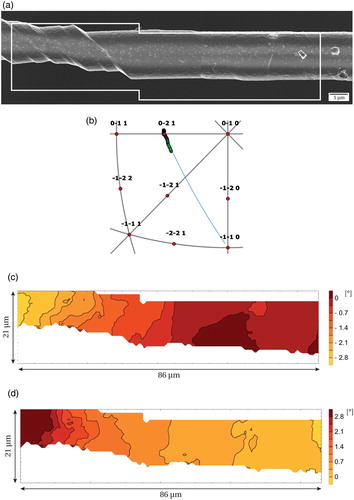
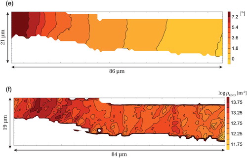
Figure 4. Streaking of 3 diffraction peaks in single-slip oriented microwire SS2 (a) around the largest visible slip step and (b) within two areas separated by a small step; window size : pixels.
Figure 5. SEM image of a deformed microwire initially oriented for multiple-slip; contour plot of misorientation angle [] (left) and dislocation density
(right).
![Figure 5. SEM image of a deformed microwire initially oriented for multiple-slip; contour plot of misorientation angle [∘] (left) and dislocation density logρGND[m−2] (right).](/cms/asset/a448122b-cb35-44f6-ac2b-dc2f3f843d10/tphm_a_1605220_f0005_oc.jpg)