Figures & data
Figure 1. Schematic of the FFS-LCD.
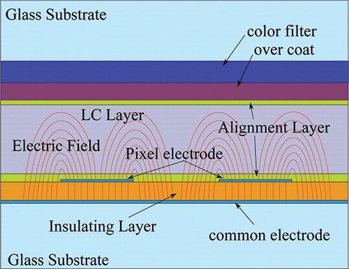
Figure 2. Two-dimensional geometric structure of the FFS-LCD created for FEM simulations using COMSOL Multiphysics.
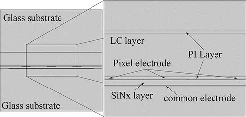
Figure 3. Enlarged view close to the electrode for the static study (a) polarization (b) charge density and current density.
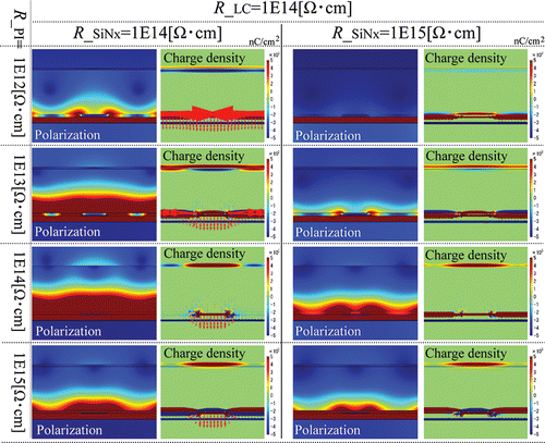
Figure 4. Charge density of the LC/PI interface.
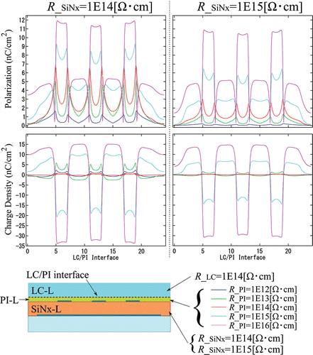
Figure 5. (a) Typical flicker wave observed in the experiments. (b) Diagrammatic illustration of the transmitted light change leading to the flicker phenomenon. Type-(A) has the same period as the driving frequency. Type (B) has half the period as the driving frequency, “Exp. 1” has a dominant type-(A), “Exp. 2” contains type-(A) and type-(B), and “Exp. 3” has a dominant type-(B).
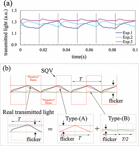
Figure 6. Typical experimental result, when a DCV (0.3 V DC, 600∼1800[s]) is applied to the CE and an SQV is applied to the PE, to enable a 20% transmittance. It is determined by the behavior of the amplitude of the flicker caused by the DCV.
![Figure 6. Typical experimental result, when a DCV (0.3 V DC, 600∼1800[s]) is applied to the CE and an SQV is applied to the PE, to enable a 20% transmittance. It is determined by the behavior of the amplitude of the flicker caused by the DCV.](/cms/asset/6d22f96e-830f-4b5e-8b1e-43a6c49bfb34/gmcl_a_1289430_f0006_oc.gif)
Figure 7. DCV applied to the CE: 0.3 V DC, 600∼1800[s], results of the dynamic study of the time evolution of the polarization and charge density. When the resistivity of (a) the LC-L is smaller than that of the PI-L, (b) the PI -L is the same as that of the LC-L and (c) the PI-L is smaller than that of the LC-L.
![Figure 7. DCV applied to the CE: 0.3 V DC, 600∼1800[s], results of the dynamic study of the time evolution of the polarization and charge density. When the resistivity of (a) the LC-L is smaller than that of the PI-L, (b) the PI -L is the same as that of the LC-L and (c) the PI-L is smaller than that of the LC-L.](/cms/asset/bd26347b-df83-4279-82a2-dd7d48091270/gmcl_a_1289430_f0007_oc.gif)
Figure 8. Snapshots of the charge density and current density, when the polarity of the SQV is reversed from negative to positive.
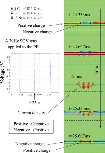
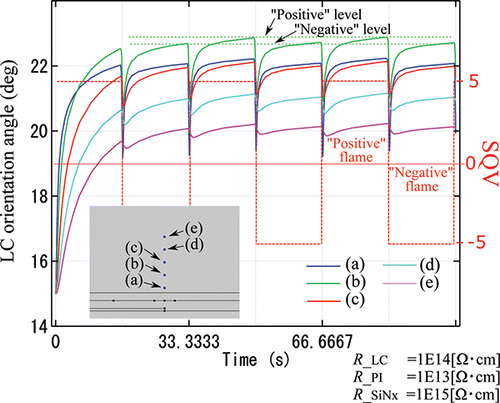
Figure 9. Time dependency of the LC molecular orientation.