
Figures & data
Figure 1. Concept of active-type photonic universal computing (APU).
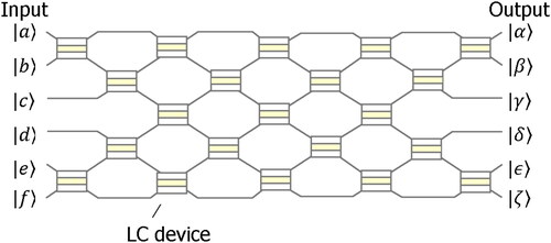
Figure 2. Overview of experimental system of Young’s interference experiment using LC phase control device. Light generated from single light source is divided by slit and is introduced into optical phase-controlled LC device [Citation26] (©2023 Liq. Cryst.).
![Figure 2. Overview of experimental system of Young’s interference experiment using LC phase control device. Light generated from single light source is divided by slit and is introduced into optical phase-controlled LC device [Citation26] (©2023 Liq. Cryst.).](/cms/asset/a4f3ef8b-1e14-4ed8-bd98-cfdf75b5bf86/gmcl_a_2342610_f0002_b.jpg)
Figure 3. Optical configuration with double slits. The configuration can be changed into two regions after passing through the slits. is distance between two slits,
is aperture length of slit,
is distance between slit and screen,
is distance from center on screen (©2023 Liq. Cryst.).
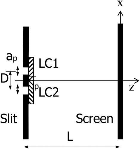
Figure 4. Device fabrication process under study. Here, self-alignment structure is formed in which the distance between slit and LC is kept close to ideal limit [Citation26] (©2023 Liq. Cryst.).
![Figure 4. Device fabrication process under study. Here, self-alignment structure is formed in which the distance between slit and LC is kept close to ideal limit [Citation26] (©2023 Liq. Cryst.).](/cms/asset/1072e381-a91f-48ab-b129-e80c5285fffb/gmcl_a_2342610_f0004_b.jpg)
Figure 5. Difference in optical configuration between control device studied before starting of this research work and self-aligned optical phase control LC device [Citation26] (©2023 Liq. Cryst.).
![Figure 5. Difference in optical configuration between control device studied before starting of this research work and self-aligned optical phase control LC device [Citation26] (©2023 Liq. Cryst.).](/cms/asset/0b631c3d-5e09-403f-859b-5aa7111eafbc/gmcl_a_2342610_f0005_b.jpg)
Figure 6. Oblique evaporation method with divided two different alignment regions. Orientation film formation area was pattern segmented by photoresist (©2023 Liq. Cryst.).
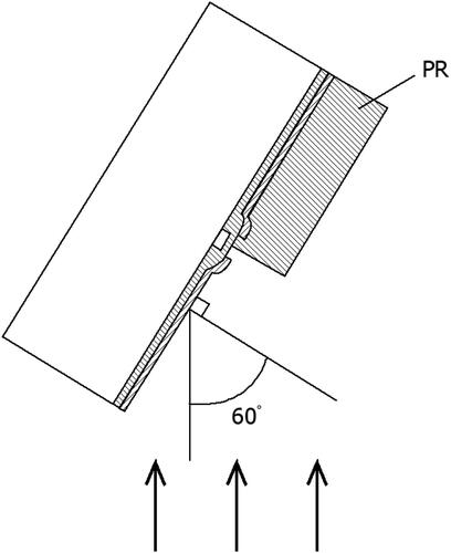
Figure 7. Complete fabrication of cell structure. Upper figure shows exterior appearance of LC cell and lower figure shows oblique evaporation directions for top and bottom substrates of LC cell [Citation26] (©2023 Liq. Cryst.).
![Figure 7. Complete fabrication of cell structure. Upper figure shows exterior appearance of LC cell and lower figure shows oblique evaporation directions for top and bottom substrates of LC cell [Citation26] (©2023 Liq. Cryst.).](/cms/asset/bf998a55-b9d3-45d8-a2b7-e01e6cd963c6/gmcl_a_2342610_f0007_b.jpg)
Figure 8. Measurement system of Young’s interference experiment. Light source under study is He-Ne laser light at wavelength of 632.8 nm. LC cell placed at center of slit and diffraction pattern of light after passing through LC device was measured using single-lens reflex camera with neutral density (ND) filter (©2023 Liq. Cryst.).
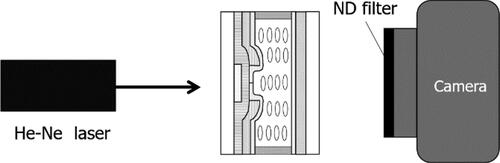
Figure 9. Simulation result of Young’s interference experiment of optical phase control LC device. Horizontal axis was normalized using value and vertical axis show intensity of outgoing light [Citation26] (©2023 Liq. Cryst.).
![Figure 9. Simulation result of Young’s interference experiment of optical phase control LC device. Horizontal axis was normalized using value ξ=xap/λL and vertical axis show intensity of outgoing light [Citation26] (©2023 Liq. Cryst.).](/cms/asset/b9f9883f-a4f9-4aaa-a0d2-d0df526919b3/gmcl_a_2342610_f0009_b.jpg)
Figure 10. Transmittance vs voltage characteristics at one of LC region under polarization microscope. Filled circles and open circles are case of under parallel nicols and crossed nicols, respectively [Citation26] (©2023 Liq. Cryst.).
![Figure 10. Transmittance vs voltage characteristics at one of LC region under polarization microscope. Filled circles and open circles are case of under parallel nicols and crossed nicols, respectively [Citation26] (©2023 Liq. Cryst.).](/cms/asset/08062076-cbf6-4fe3-aa4b-daae6eddc974/gmcl_a_2342610_f0010_b.jpg)
Figure 11. Photograph of interference fringes patterns, where (a) is 0 V, (b) is 2 V, (c) is 2.5 V, (d) is 3 V, (e) is 4 V, and (f) is 9 V condition [Citation26] (©2023 Liq. Cryst.).
![Figure 11. Photograph of interference fringes patterns, where (a) is 0 V, (b) is 2 V, (c) is 2.5 V, (d) is 3 V, (e) is 4 V, and (f) is 9 V condition [Citation26] (©2023 Liq. Cryst.).](/cms/asset/bf952975-901f-40aa-9cfb-1d1dc15b70d8/gmcl_a_2342610_f0011_b.jpg)
Figure 12. Typical interference pattern with converted to eight-bit gray level at the horizontal line [Citation26] (©2023 Liq. Cryst.).
![Figure 12. Typical interference pattern with converted to eight-bit gray level at the horizontal line [Citation26] (©2023 Liq. Cryst.).](/cms/asset/6da9623a-ab5d-4301-b58c-ef9495c6bf18/gmcl_a_2342610_f0012_b.jpg)
Figure 13. Logic operation of position a and b for "0" and "1" points. Applied voltages are among 0, 2.5 and 9 V. Where point A and B corresponds to distance value at −1,297 and −1,034, respectively [Citation26] (©2023 Liq. Cryst.).
![Figure 13. Logic operation of position a and b for "0" and "1" points. Applied voltages are among 0, 2.5 and 9 V. Where point A and B corresponds to distance value at −1,297 and −1,034, respectively [Citation26] (©2023 Liq. Cryst.).](/cms/asset/62aaa03b-a557-4ec4-9cf9-f77b3eb3ff52/gmcl_a_2342610_f0013_c.jpg)
Figure 14. Optical configuration of a beam splitter with the input-output relations in the Heisenberg picture. The beam splitter used is a liquid crystal retarder under study [Citation46] (©2024 JJAP).
![Figure 14. Optical configuration of a beam splitter with the input-output relations in the Heisenberg picture. The beam splitter used is a liquid crystal retarder under study [Citation46] (©2024 JJAP).](/cms/asset/4783a325-f2ba-4934-bd7c-667da24305b7/gmcl_a_2342610_f0014_c.jpg)
Figure 15. Image of liquid crystal director configuration. Where the initial condition of the LC director at z = 0 and z = d is tilted to a pretilt angle, the electric field is applied to the z direction. Under voltage application above threshold voltage Vth, director deformation has occurred (©2024 JJAP).
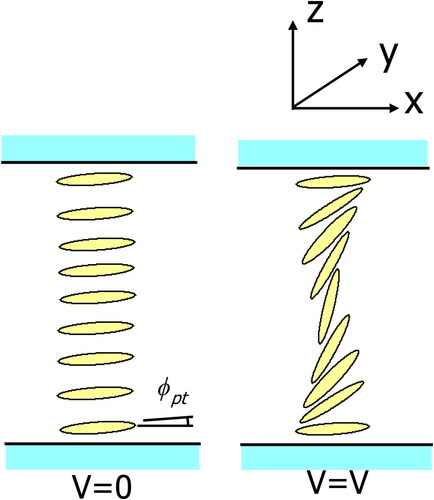
Figure 16. Image of Hamiltonian and eigenvalue of energy at state Photon number of operator
is introduced [Citation46] (©2024 JJAP).
![Figure 16. Image of Hamiltonian and eigenvalue of energy at state |n. Photon number of operator n̂, n̂=â†â is introduced [Citation46] (©2024 JJAP).](/cms/asset/1a32eb37-007d-4ced-9152-7b11494fc59a/gmcl_a_2342610_f0016_b.jpg)
Figure 17. Quantum circuit form for linear optics of beam splitter (©2024 JJAP).
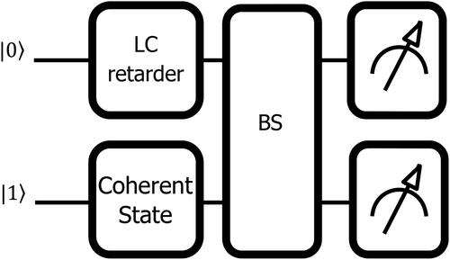
Figure 18. Calculated director deformation under voltage application. The applied voltage is 2, 4, 6, 8, and 10 V where the division number of liquid crystal cells is 1,000 [Citation46] (©2024 JJAP).
![Figure 18. Calculated director deformation under voltage application. The applied voltage is 2, 4, 6, 8, and 10 V where the division number of liquid crystal cells is 1,000 [Citation46] (©2024 JJAP).](/cms/asset/87009493-746d-420d-8b54-b3c4b539c6c3/gmcl_a_2342610_f0018_b.jpg)
Figure 19. Calculation result of retardation by changing voltage. The vertical axis is retardation variation where n is the actual refractive index, d is cell thickness and λ is the wavelength of light. Insets of the figure are director profiles at voltages of 2, 4, 6, and 8 V [Citation46] (©2024 JJAP).
![Figure 19. Calculation result of retardation by changing voltage. The vertical axis is retardation variation nd/λ, where n is the actual refractive index, d is cell thickness and λ is the wavelength of light. Insets of the figure are director profiles at voltages of 2, 4, 6, and 8 V [Citation46] (©2024 JJAP).](/cms/asset/c95d5785-c1d7-4d76-bb98-2cc9fb322b24/gmcl_a_2342610_f0019_b.jpg)
Figure 20. Intensity vs. voltage characteristics for the classical case, amplitude α1 = 1 [Citation46] (©2024 JJAP).
![Figure 20. Intensity vs. voltage characteristics for the classical case, amplitude α1 = 1 [Citation46] (©2024 JJAP).](/cms/asset/e8b9aaa8-b2cd-4b7e-a24a-d240dcfd33d6/gmcl_a_2342610_f0020_b.jpg)
Figure 21. Intensity vs voltage characteristics for amplitude of intensity α1 = 6.3 × 10⁻¹⁰ [Citation46] (©2024 JJAP).
![Figure 21. Intensity vs voltage characteristics for amplitude of intensity α1 = 6.3 × 10⁻¹⁰ [Citation46] (©2024 JJAP).](/cms/asset/acdb99cf-1f26-44e7-8a55-ccc30ab091a9/gmcl_a_2342610_f0021_b.jpg)
Figure 22. Intensity vs voltage characteristics for amplitude of intensity α1 = 2.6 × 10⁻¹⁰ [Citation46] (©2024 JJAP).
![Figure 22. Intensity vs voltage characteristics for amplitude of intensity α1 = 2.6 × 10⁻¹⁰ [Citation46] (©2024 JJAP).](/cms/asset/cdca5b42-aae6-4cbf-aba2-57f95c1c242c/gmcl_a_2342610_f0022_b.jpg)
Figure 23. Intensity vs voltage characteristics for amplitude of intensity α1 = 2.0 × 10⁻¹⁰ [Citation46] (©2024 JJAP).
![Figure 23. Intensity vs voltage characteristics for amplitude of intensity α1 = 2.0 × 10⁻¹⁰ [Citation46] (©2024 JJAP).](/cms/asset/1f6e05dd-9d1e-4d63-bd3f-76e780a6c57e/gmcl_a_2342610_f0023_b.jpg)
Figure 24. Optical experiment system under study. Laser: He-Ne Laser (632.8 nm); BS: Beam splitter; M: Mirror; TN: Twisted Nematic LC (©2024 JJAP).
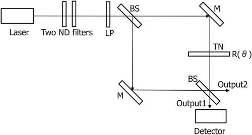
Figure 25. Simulation results of interference light intensity [Citation38] (©2024 JJAP).
![Figure 25. Simulation results of interference light intensity [Citation38] (©2024 JJAP).](/cms/asset/e4419112-9077-4ffd-b107-69dfd95b6f00/gmcl_a_2342610_f0025_b.jpg)
Figure 26. Configuration of TN liquid crystal cell.
Figure 27. Shape of ITO pattern after ITO electrodes were etched (©2024 JJAP).
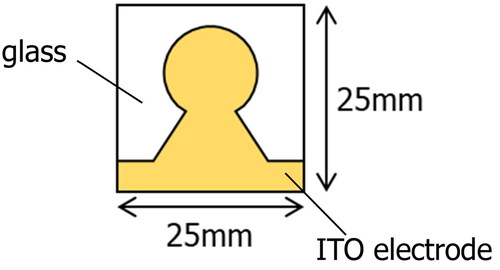
Figure 28. Voltage vs transmittance of TN LC device under study [Citation38] (©2024 JJAP).
![Figure 28. Voltage vs transmittance of TN LC device under study [Citation38] (©2024 JJAP).](/cms/asset/b4da7fda-86d0-4d34-879d-78ccb97035fa/gmcl_a_2342610_f0028_b.jpg)
Figure 29. Change in the pattern of interfering light due to the application of voltage to the LC device [Citation29] (©2024 JJAP).
![Figure 29. Change in the pattern of interfering light due to the application of voltage to the LC device [Citation29] (©2024 JJAP).](/cms/asset/e9553d5b-9e5a-4dbb-9fac-d7d469daedab/gmcl_a_2342610_f0029_b.jpg)
Figure 30. Number of photons vs voltage characteristics [Citation38] (©2024 JJAP).
![Figure 30. Number of photons vs voltage characteristics [Citation38] (©2024 JJAP).](/cms/asset/f37753ea-0c99-4c2b-8074-dc24a4b46fa8/gmcl_a_2342610_f0030_b.jpg)
Figure 31. Schematic diagram of 2-bit linear optical quantum computer [Citation55] (©2024 JJAP).
![Figure 31. Schematic diagram of 2-bit linear optical quantum computer [Citation55] (©2024 JJAP).](/cms/asset/6fe03533-b738-4a86-ad08-01bddad370d2/gmcl_a_2342610_f0031_b.jpg)
Figure 32. Phase state of light at each light path and output [Citation55] (©2024 JJAP).
![Figure 32. Phase state of light at each light path and output [Citation55] (©2024 JJAP).](/cms/asset/4317697f-0f0e-4154-9484-969e89734041/gmcl_a_2342610_f0032_b.jpg)
Figure 33. Device structure under study [Citation55] (©2024 JJAP).
![Figure 33. Device structure under study [Citation55] (©2024 JJAP).](/cms/asset/b892b663-4dbf-418e-a552-39ec64c91052/gmcl_a_2342610_f0033_b.jpg)
Figure 34. Transmittance vs voltage characteristics. Left, left optical rotation LC device. Right, right optical rotation LC device [Citation55] (©2024 JJAP).
![Figure 34. Transmittance vs voltage characteristics. Left, left optical rotation LC device. Right, right optical rotation LC device [Citation55] (©2024 JJAP).](/cms/asset/27bbe998-cf2e-4bed-a4fe-50063d8254d5/gmcl_a_2342610_f0034_b.jpg)
Table 1. Characteristics of LCD (right optical rotation) (©2024 JJAP).
Table 2. Characteristics of LCD (left optical rotation) (©2024 JJAP).
Figure 35. Output optical interference state at the beginning of the experiment [Citation55] (©2024 JJAP).
![Figure 35. Output optical interference state at the beginning of the experiment [Citation55] (©2024 JJAP).](/cms/asset/ff08714b-eb3c-410f-91bc-b501b1c5ff39/gmcl_a_2342610_f0035_b.jpg)
Figure 36. Output Interference light change. Input bits from left to right: "00," "01," "10," "11" [Citation55] (©2024 JJAP).
![Figure 36. Output Interference light change. Input bits from left to right: "00," "01," "10," "11" [Citation55] (©2024 JJAP).](/cms/asset/6d842c90-6b30-4a5b-9454-8d215618797c/gmcl_a_2342610_f0036_b.jpg)
Figure 37. Image analysis of output interference light [Citation55] (©2024 JJAP).
![Figure 37. Image analysis of output interference light [Citation55] (©2024 JJAP).](/cms/asset/62d0b178-5e8f-4b5e-a220-d709747f301a/gmcl_a_2342610_f0037_b.jpg)
Figure 38. Left figure is case of shutter speed 1/500 s without ND filter. Right figure is case of shutter speed 2400 s with ND filter [Citation55] (©2024 JJAP).
![Figure 38. Left figure is case of shutter speed 1/500 s without ND filter. Right figure is case of shutter speed 2400 s with ND filter [Citation55] (©2024 JJAP).](/cms/asset/1f2bf766-ee59-40dc-9ccb-917d93904508/gmcl_a_2342610_f0038_b.jpg)
Figure 39. Photon counting characteristics by changing input signal of LC cell. Input bits are switched in the order of "01," "00," "11," "10" for every 120 s [Citation55] (©2024 JJAP).
![Figure 39. Photon counting characteristics by changing input signal of LC cell. Input bits are switched in the order of "01," "00," "11," "10" for every 120 s [Citation55] (©2024 JJAP).](/cms/asset/78e44899-0615-4654-a581-d19f6eace5a4/gmcl_a_2342610_f0039_b.jpg)