Figures & data
Figure 1. (a) Schematic diagram of the experimental setup of the grating imaging technique; (b) in-plane and cross-plane heat flow generated by the pump and detected by the probe.
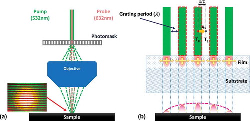
Figure 2. (a) Experimental and fitting results for Cu 220-nm-thick nano-film measured by ns-TDTR (λ = ∞) and NGI with grating periods of 10 μm and 20 μm; (b) comparison of κx of Cu nano-films measured by NGI with four-point probe results as well as reference values. (Error bars indicate a standard deviation based on five measurements at different locations on the sample.)
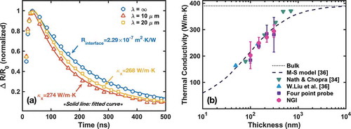
Figure 3. (a) Experimental and fitting results for an 8 nm x 8 nm GaAs/AlAs SL with grating periods of 6and 9
; (b) in-plane thermal conductivity results with different grating periods (error bars indicate a standard deviation based on five measurements at different locations on the sample); (c) sensitivity analysis of all parameters; (d) uncertainty for in-plane thermal conductivity measurement using NGI with a grating period of 7
.
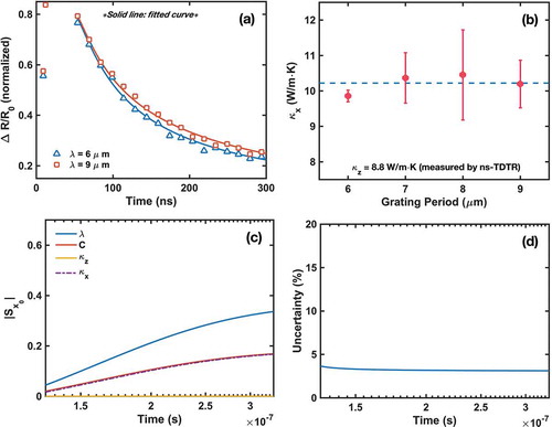
Figure 4. (a) Sensitivity analysis of all parameters for 220 nm Cu on Si measured with NGI; (b) uncertainty of measured with NGI; (c) sensitivity analysis of all parameters for 220 nm Cu on Si measured with ns-TDTR; (d) uncertainty of interface resistance measured with ns-TDTR.
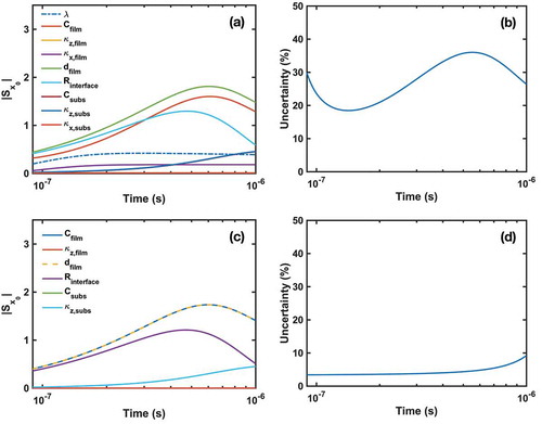
Figure 5. Sensitivity analysis for 220 nm Cu on various substrates: (a) Si; (b) AlAs; (c) GaAs; (d) Si3N4; (e) SiO2; and (f) PMMA. (g) Uncertainty of κx,film measurement in a 220 nm Cu film on various substrates.
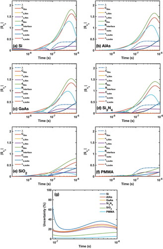
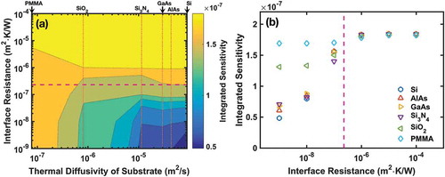
Figure 6. Sensitivity for Cu on various substrates with different interface resistance values. (Purple dashed horizontal line: used value for 220 nm Cu on Si.).