Figures & data
Figure 1. Structure of the complementary inverter.
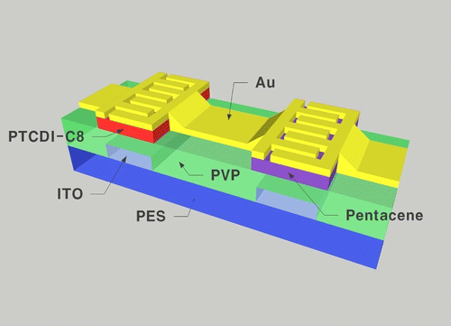
Figure 2. Transfer curves of (a) pentacene and (b) PTCDI-C8 transistors.
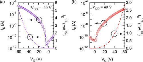
Figure 3. (a) Schematic diagram of a complementary inverter. (b) Output characteristics of the complementary inverter: V IN−V OUT transfer curves (solid line) and gains (dashed line).
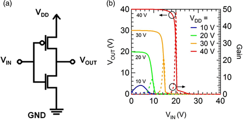
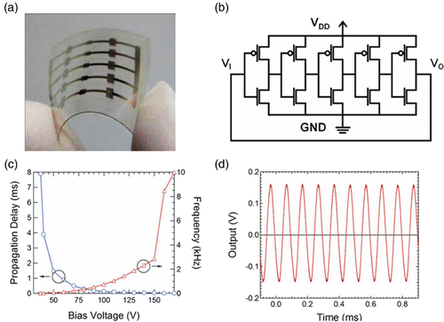
Figure 4. (a) An image of the five-stage ring oscillator on the flexible PES substrate (PES). (b) Schematic diagram of the five-stage ring oscillator. (c) Characteristics of the propagation delay in the one-stage inverter, and output frequency of the ring oscillator versus bias voltage. (d) The output signal of the five-stage ring oscillator at V DD=−170 V shows f OSC=10 kHz.