Figures & data
Figure 1. Device structures of the conventional OLED and the iOLED, respectively.
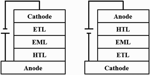
Figure 2. J–V characteristics of electron-only devices depending on the different deposition sequences of a thin LiF interlayer. [Reprinted with permission from Heil et al. Citation44, © 2001, American Institute of Physics.]
![Figure 2. J–V characteristics of electron-only devices depending on the different deposition sequences of a thin LiF interlayer. [Reprinted with permission from Heil et al. Citation44, © 2001, American Institute of Physics.]](/cms/asset/b7523f5c-414f-41ae-bcde-cafdfa3eccf8/tjid_a_779324_o_f0002g.jpg)
Figure 3. Energy level diagrams of doped organic layers obtained via (a) UPS, (b) KP, and (c) C−V measurements, respectively. [Reprinted from Blochwitz et al. Citation57, © 2001, with permission from Elsevier; Kröger et al. Citation73, © 2007 by American Physical Society; and Lee et al. Citation74, © 2012, Wiley-VCH.]
![Figure 3. Energy level diagrams of doped organic layers obtained via (a) UPS, (b) KP, and (c) C−V measurements, respectively. [Reprinted from Blochwitz et al. Citation57, © 2001, with permission from Elsevier; Kröger et al. Citation73, © 2007 by American Physical Society; and Lee et al. Citation74, © 2012, Wiley-VCH.]](/cms/asset/eee35ed6-a939-444e-b302-6a17b066f702/tjid_a_779324_o_f0003g.gif)
Figure 4. Change in the energy barrier at the M/O interface by controlling the orientation of the organic material. Energy level diagram for the (a) standing-6T/standing-DH6T/lying-DH6T-monolayer/Ag(111) structure, and (b) ITO/ZnPc/C60 and ITO/CuI/ZnPc/C60. [Reprinted from Duhm et al. Citation82, © 2008, with permission from Macmillan Publishers, Ltd. and Kim et al. Citation86, © 2013, with permission from Elsevier.]
![Figure 4. Change in the energy barrier at the M/O interface by controlling the orientation of the organic material. Energy level diagram for the (a) standing-6T/standing-DH6T/lying-DH6T-monolayer/Ag(111) structure, and (b) ITO/ZnPc/C60 and ITO/CuI/ZnPc/C60. [Reprinted from Duhm et al. Citation82, © 2008, with permission from Macmillan Publishers, Ltd. and Kim et al. Citation86, © 2013, with permission from Elsevier.]](/cms/asset/4401ffe2-29be-4718-a645-0a4469a38aff/tjid_a_779324_o_f0004g.jpg)
Figure 5. Device performances of three different iOLEDs, using the B3PYMPM, Bphen, and TPBi homo-junctions, respectively. (a) Current J–V–L characteristics and (b) quantum efficiency-luminance (η-L) characteristics of the iOLEDs. [Reprinted from Lee et al. Citation27, © 2011, with permission from Elsevier.]
![Figure 5. Device performances of three different iOLEDs, using the B3PYMPM, Bphen, and TPBi homo-junctions, respectively. (a) Current J–V–L characteristics and (b) quantum efficiency-luminance (η-L) characteristics of the iOLEDs. [Reprinted from Lee et al. Citation27, © 2011, with permission from Elsevier.]](/cms/asset/84be8da6-be6f-4983-a645-f8095195d173/tjid_a_779324_o_f0005g.jpg)
Table 1. Performances of the iOLEDs, using three different homo-junctions. The operating voltage at injection and turn-on, the EQE at maximum and 1000 cd/m2, and the power efficiency at maximum and 1000 cd/m2 are listed, respectively. [Reprinted from Lee et al. Citation27, © 2011, with permission from Elsevier.]
Figure 6. J–V characteristics of electron-only devices with inverted structures of (a) ITO/Rb2CO3-doped ETL (50 m, 15 wt%)/Al (open symbol) or (b) ITO/Rb2CO3-doped ETL (20 m, 15 wt%)/undoped ETL (30 nm)/Al (solid symbol). [Reprinted from Lee et al. Citation27, © 2011, with permission from Elsevier.]
![Figure 6. J–V characteristics of electron-only devices with inverted structures of (a) ITO/Rb2CO3-doped ETL (50 m, 15 wt%)/Al (open symbol) or (b) ITO/Rb2CO3-doped ETL (20 m, 15 wt%)/undoped ETL (30 nm)/Al (solid symbol). [Reprinted from Lee et al. Citation27, © 2011, with permission from Elsevier.]](/cms/asset/a3934d02-1df3-4cc1-8590-1ce866b4b21f/tjid_a_779324_o_f0006g.jpg)
Figure 7. Energy level diagrams of (a) ITO/n-B3PYMPM/ B3PYMPM, (b) ITO/n-Bphen/Bphen, and (c) ITO/n-TPBi/ TPBi, respectively, obtained via UPS measurement. [Reprinted from Lee et al. Citation27, © 2011, with permission from Elsevier.]
![Figure 7. Energy level diagrams of (a) ITO/n-B3PYMPM/ B3PYMPM, (b) ITO/n-Bphen/Bphen, and (c) ITO/n-TPBi/ TPBi, respectively, obtained via UPS measurement. [Reprinted from Lee et al. Citation27, © 2011, with permission from Elsevier.]](/cms/asset/2ecc011f-f3b8-4e54-b85f-ac920bdada95/tjid_a_779324_o_f0007g.jpg)
Figure 8. Device structures of three different iOLEDs with the B3PYMPM homo-junction, n-B3PYMPM/Bphen hetero-junction, and n-B3PYMPM/TPBi hetero-junction, respectively.
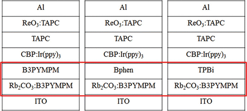
Figure 9. Device performances of three different iOLEDs with the n-B3PYMPM/B3PYMPM homo-junction, n-B3PYMPM/Bphen hetero-junction, and n-B3PYMPM/TPBi hetero-junction as the ETL, respectively. (a) J–V–L and (b) η-L characteristics of the iOLEDs.
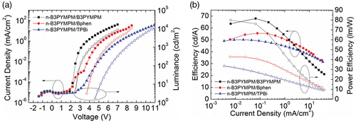
Figure 10. Device structure of the iOLED using the organic p–n junction as an electron injection and electron-transporting layer, and J–V characteristics of the organic p–n junction composed of p-CuPc/n-Bphen. [Reprinted from Lee et al. Citation116, © 2012, with permission from Elsevier.]
![Figure 10. Device structure of the iOLED using the organic p–n junction as an electron injection and electron-transporting layer, and J–V characteristics of the organic p–n junction composed of p-CuPc/n-Bphen. [Reprinted from Lee et al. Citation116, © 2012, with permission from Elsevier.]](/cms/asset/7a86847a-90c2-4ce0-975e-f78775ba2a4c/tjid_a_779324_o_f0010g.jpg)
Figure 11. Device performances of five different iOLEDs depending on the work function of the bottom cathode. (a) J–V and (b) current density–luminance (L−V) characteristics of the iOLEDs, and the value of the work function of the bottom cathode therein. [Reprinted from Lee et al. Citation116, © 2012, with permission from Elsevier.]
![Figure 11. Device performances of five different iOLEDs depending on the work function of the bottom cathode. (a) J–V and (b) current density–luminance (L−V) characteristics of the iOLEDs, and the value of the work function of the bottom cathode therein. [Reprinted from Lee et al. Citation116, © 2012, with permission from Elsevier.]](/cms/asset/04731efc-b960-43d0-a060-ee6ea8227c61/tjid_a_779324_o_f0011g.jpg)