Figures & data
Figure 1. Diagram of the MB7 structure: (a) conventional array and (b) vertically placed pixel array.
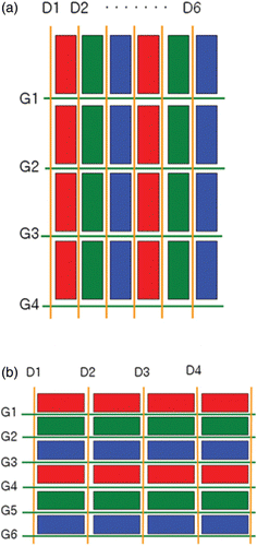
Figure 2. CS type for the MB7 structure.
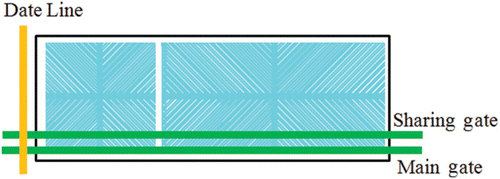
Figure 3. Eight-domain driving for the improvement of the off-axis image quality in the VA mode.
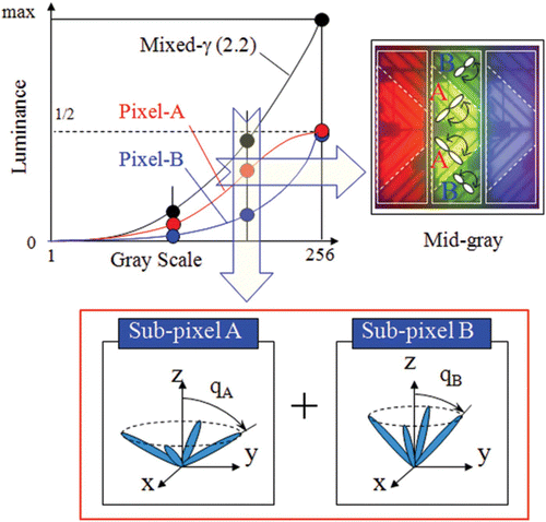
Figure 4. Pixel circuit for the RD type: (a) equivalent circuit and (b) diagram for operation.
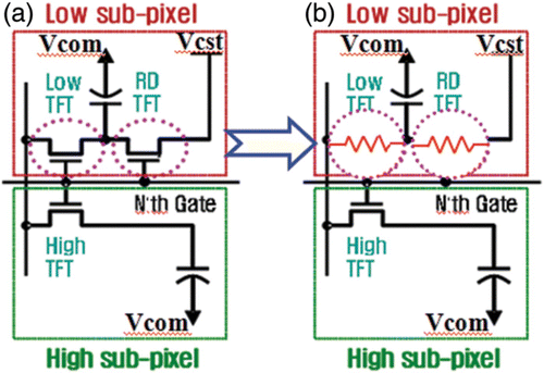
Figure 5. Simulation schematic and charging properties for the RD type: (a) schematic for simulation and (b) charging properties of the subpixels.
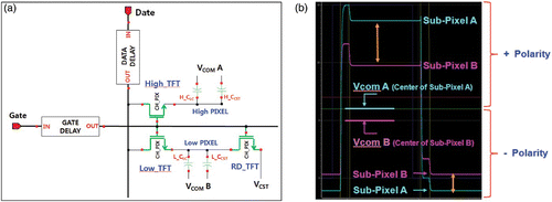
Figure 6. Voltage ration simulation results of subpixel B: (a) voltage ratio from gray in the Vcst level and (b) Vcst influence from the RD-TFT size.
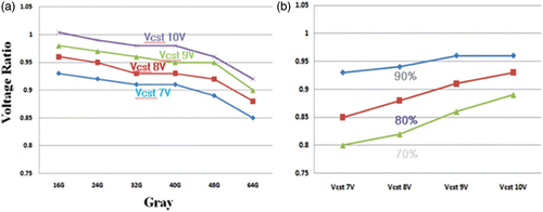
Table 1. Prototype evaluation results.
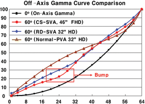
Figure 7. Off-axis gamma comparison.