Figures & data
Figure 1. (a) Cross-sectional scheme and (b) optical micrograph of SA a-IGZO TFTs.
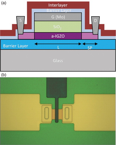
Figure 2. (a) Transfer (VGS−IDS) and (b) output (VDS−IDS) characteristics of SA TFTs with W = 15 µm, L = 5 µm, and SP = 10 µm.
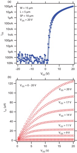
Figure 3. Dependence of the RSHEET of hydrogen plasma, Ar plasma, and Ca-treated a-IGZO on the channel length at V = 2.0 V. The layout of the resistor structure is shown in the inset.
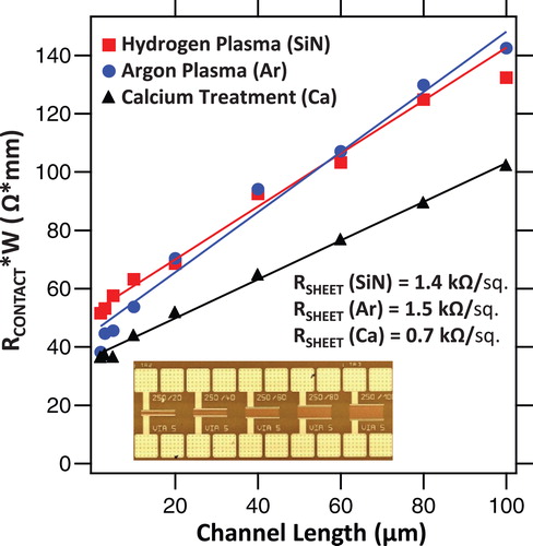
Figure 4. Transfer (VGS−IDS) characteristics dependence on (a) ‘L’ scaling and (b) ‘SP’ scaling of SA TFTs.
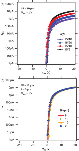
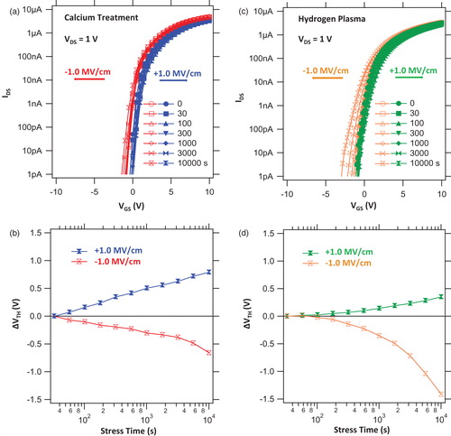
Figure 5. (a and c) Evolution of the transfer characteristics (VGS−IDS) of SA TFTs (W = 15 µm and L = 5 µm) as a function of the duration time at +1.0 MV/cm (VGS = +20 V and VDS = 0 V) and at −1.0 MV/cm (VGS = −20 V and VDS = 0 V). (b and d) VTH shift as a function of the stress time in the positive and negative directions.