Figures & data
Figure 1. Schematic diagram of the e-beam system.
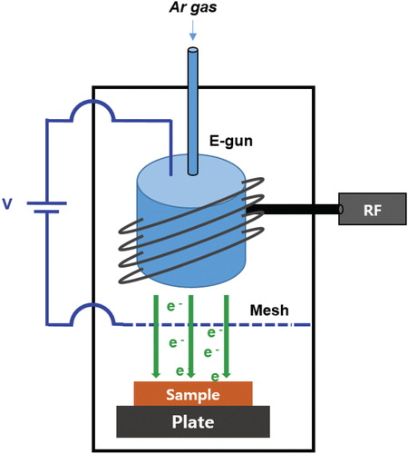
Table 1. Electron beam exposure conditions.
Figure 2. Images obtained before and after the e-beam exposure of the a-Si:H thin films deposited via PECVD and sputtering: (a) sputter-deposited a-Si:H thin film; (b) sputter-deposited silicon thin film after e-beam exposure; (c) PECVD a-Si:H thin film; and (d) PECVD silicon thin film after e-beam exposure.
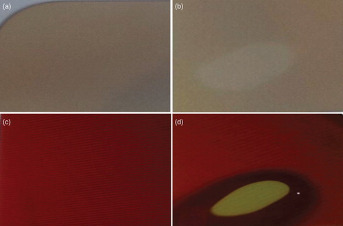
Figure 3. SEM images of the silicon thin films after e-beam exposure: (a) sputter-deposited silicon thin film; (b) sputter-deposited silicon thin film with thermal annealing; (c) PECVD silicon thin film; and (d) PECVD silicon thin film with thermal annealing.
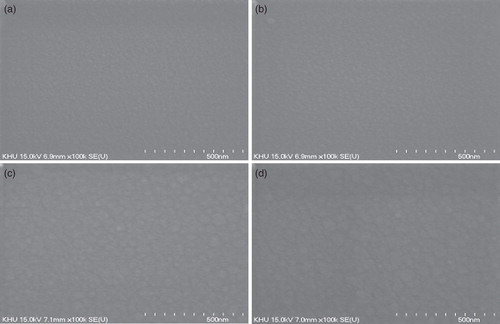
Figure 4. XRD patterns of the silicon thin films after crystallization via e-beam exposure.
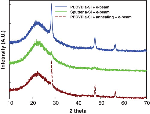
Figure 5. Raman spectra of the silicon thin films after crystallization via e-beam exposure.
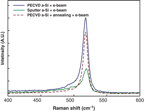
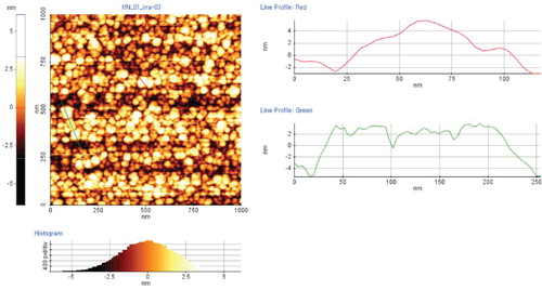
Figure 6. AFM image and roughness of the PECVD silicon thin film after e-beam exposure.