Figures & data
Figure 1. (a) PMOS 6T1C Vth compensation pixel circuit in Ref. [Citation1]; (b) its timing diagram.
![Figure 1. (a) PMOS 6T1C Vth compensation pixel circuit in Ref. [Citation1]; (b) its timing diagram.](/cms/asset/6d9af6f3-69a1-4680-adde-9a5fa5030186/tjid_a_1259128_f0001_c.jpg)
Figure 2. (a) Initializing phase, (b) programing phase, and (c) emission phase of the 6T1C circuit operation process.
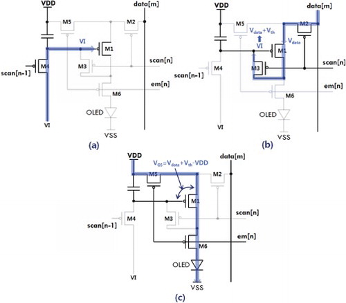
Figure 3. Waveforms of the gate and source voltages of M1 TFT during the operation phases for the different mobility cases.
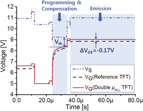
Table 1. RPI poly-Si TFT model parameters for spice simulation.
Figure 4. Transfer characteristics of the TFT models for (a) high-field mobility (MU0) doubling, (b) low-field mobility (MU1) doubling, (c) subthreshold mobility (MUS) doubling, and (d) all the mobilities’ (MU0, MU1, and MUS) doubling when VDS = −10 V and TFT’s W/L = 2 μm/10 μm.
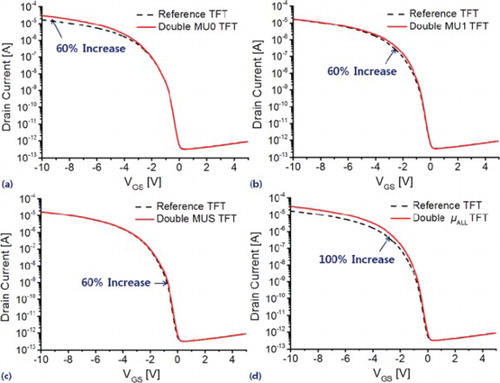
Figure 5. Effects of all the mobilities’ doubling on the programed |VGS.M1| values, and resultant OLED currents vs. the various target currents.
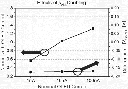
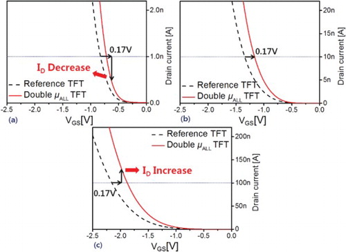
Figure 6. Different effects of the programed |VGS.M1| decrease on the OLED currents for various target currents: (a) 1 nA; (b) 10 nA; and (c) 100 nA.