
Figures & data
Figure 1. Local geometry and interfacial curvature described by mean and Gaussian curvatures (H, K).
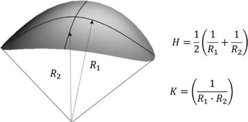
Figure 2. Schematic representation of molecular orientations of (a) smectic A phase and (b) smectic C phase. (c) Molecular structure of bent core LC known as NOBOW. The molecule has an inherent polar direction p and the tilt of the molecular plane, n, from the layer normal, s. (d) The scheme and transmission electron micrograph of the helical nano filament, having 5–8 twisted smectic layers of layer distance, d ∼ 4.5 nm, width of filament, w ∼ 35 nm and the half pitch, hp ∼ 110 nm. The layer edge (LE) region and layer surface (LS) region were observed by Kim et al. [Citation77].
![Figure 2. Schematic representation of molecular orientations of (a) smectic A phase and (b) smectic C phase. (c) Molecular structure of bent core LC known as NOBOW. The molecule has an inherent polar direction p and the tilt of the molecular plane, n, from the layer normal, s. (d) The scheme and transmission electron micrograph of the helical nano filament, having 5–8 twisted smectic layers of layer distance, d ∼ 4.5 nm, width of filament, w ∼ 35 nm and the half pitch, hp ∼ 110 nm. The layer edge (LE) region and layer surface (LS) region were observed by Kim et al. [Citation77].](/cms/asset/fc91dab4-a69d-4cde-a157-5e0f722c9b1a/tjid_a_1410500_f0002_c.jpg)
Figure 3. (a) Schematic illustration of a set of parallel layers Si, their normal n, the loci of centers of curvature C1 and C2, the focal surfaces F1 and F2. (b) The focal surfaces reduced into two conjugated line of ellipse and hyperbola by forming cyclides. The straight lines are layer normal vectors in the cyclides. Schematic sketches of (c) FCD-type 1, (d) FCD-type 2, and (e) FCD-type 3 [Citation27].
![Figure 3. (a) Schematic illustration of a set of parallel layers Si, their normal n, the loci of centers of curvature C1 and C2, the focal surfaces F1 and F2. (b) The focal surfaces reduced into two conjugated line of ellipse and hyperbola by forming cyclides. The straight lines are layer normal vectors in the cyclides. Schematic sketches of (c) FCD-type 1, (d) FCD-type 2, and (e) FCD-type 3 [Citation27].](/cms/asset/19b2c907-e22c-4d42-bcfe-73ff09b0e901/tjid_a_1410500_f0003_c.jpg)
Figure 4. (a) Diagram of a single TFCD cross-section. R1 and R2 are the principal radii of layer curvatures. The LC molecules are aligned along the layer normal line such as that connect the point of straight line defect with the point of circular line. Every layer adopts the negative Gaussian curvature, K = R1·R2 < 0. a is the radius of the TFCD. (b) Top-view SEM image of the TFCD film in equilibrium with hexagonal arrangement. The inset depicts the POM image corresponding to the TFCD, showing the projection of radial orientation of LC molecules at the basis of TFCD. (c–e) POM and SEM images (left column and right column, respectively) of TFCDs in microchannels of different depths h = 2, 5, 10 µm, and fixed width ∼50 µm [Citation47].
![Figure 4. (a) Diagram of a single TFCD cross-section. R1 and R2 are the principal radii of layer curvatures. The LC molecules are aligned along the layer normal line such as that connect the point of straight line defect with the point of circular line. Every layer adopts the negative Gaussian curvature, K = R1·R2 < 0. a is the radius of the TFCD. (b) Top-view SEM image of the TFCD film in equilibrium with hexagonal arrangement. The inset depicts the POM image corresponding to the TFCD, showing the projection of radial orientation of LC molecules at the basis of TFCD. (c–e) POM and SEM images (left column and right column, respectively) of TFCDs in microchannels of different depths h = 2, 5, 10 µm, and fixed width ∼50 µm [Citation47].](/cms/asset/7f4cea40-f5fd-4523-839f-3f008967c60e/tjid_a_1410500_f0004_c.jpg)
Figure 5. Sublimation and recondensation in nature (a) Frost on a leaf. (b) Sketches of the process of merging ice cubes in humid conditions. (c) Geyserite at Crater Hills Geyser, formed wherever relatively alkaline hot springs percolate out of the ground.
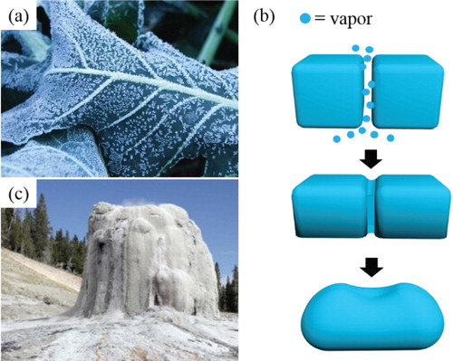
Figure 6. TGA of LC materials. (a) Chemical structures of Y001–Y006. (b) TGA plots for Y001–Y006 as a function of temperature during heating (heating rate: 1°C/min) shows that sublimation of Y001–Y004 occurs before the material reaches their respective isotropic temperatures; Y005 and Y006 show no sublimation in the SmA phase [Citation68].
![Figure 6. TGA of LC materials. (a) Chemical structures of Y001–Y006. (b) TGA plots for Y001–Y006 as a function of temperature during heating (heating rate: 1°C/min) shows that sublimation of Y001–Y004 occurs before the material reaches their respective isotropic temperatures; Y005 and Y006 show no sublimation in the SmA phase [Citation68].](/cms/asset/a33aa742-e1f5-4d0e-8435-50525b6e8d70/tjid_a_1410500_f0006_c.jpg)
Table 1. Phase transition temperatures of materials during cooling at a rate 5°C/min (Cr = crystal, SmE = smectic E, SmA = smectic A, I = isotropic phase) [Citation68].
Figure 7. Morphology changes of TFCDs during the sintering process. POM textures of TFCD film subject to thermal sublimation at 180°C as a function of time. (a) 0 min, (d) 6 min, (g) 12 min. SEM images of the evolved LC films during sintering and their cross-sectional schemes; (b,c) original TFCDs. (e,f) Dome-like structures. (h,i) Concentric tori patterns with pyramidal dome shape. The film thickness is reduced from ∼5 to <2 µm during the process [Citation67].
![Figure 7. Morphology changes of TFCDs during the sintering process. POM textures of TFCD film subject to thermal sublimation at 180°C as a function of time. (a) 0 min, (d) 6 min, (g) 12 min. SEM images of the evolved LC films during sintering and their cross-sectional schemes; (b,c) original TFCDs. (e,f) Dome-like structures. (h,i) Concentric tori patterns with pyramidal dome shape. The film thickness is reduced from ∼5 to <2 µm during the process [Citation67].](/cms/asset/0ec1aa05-5b42-4e78-8778-3aef72dab245/tjid_a_1410500_f0007_c.jpg)
Figure 8. Sintering diagram of morphological changes of the SmLC films. Eight distinct types of resulting structures as a function of sintering temperatures and times. (1) TFCDs, (2) TFCDs with caps, (3) conical pyramid with depressions, (4) Conical pyramid with caps, (5) concentric patterns with depressions, (6) concentric patterns with caps in centers, (7) Udumbara flower, and (8) Domes. Each structure is marked by a colored box in the diagram and its SEM image is displayed under the diagram [Citation68].
![Figure 8. Sintering diagram of morphological changes of the SmLC films. Eight distinct types of resulting structures as a function of sintering temperatures and times. (1) TFCDs, (2) TFCDs with caps, (3) conical pyramid with depressions, (4) Conical pyramid with caps, (5) concentric patterns with depressions, (6) concentric patterns with caps in centers, (7) Udumbara flower, and (8) Domes. Each structure is marked by a colored box in the diagram and its SEM image is displayed under the diagram [Citation68].](/cms/asset/d6e0807f-a446-4fa9-b860-5c343daa7514/tjid_a_1410500_f0008_c.jpg)
Figure 9. SEM images corresponding to the sintering diagram [Citation68].
![Figure 9. SEM images corresponding to the sintering diagram [Citation68].](/cms/asset/df19ef85-f796-4e8d-a010-92a5d110bb8d/tjid_a_1410500_f0009_c.jpg)
Figure 10. Reconstruction of layering in the smectic films during thermal sintering. (a) The mean curvature within the TFCD varies along with ρ from negative inside the cylinder of radius r = a/2 to positive within the region a/2 < r < a. (b) Excess sublimation rate (arbitrary units) versus normalized distance ρ/a from the TFCD axis for three ratio of film thickness (h/a) = 0.5; 1; 2. (c) Harmonious inosculation of equidistant layers between a TFCD remnant with K < 0 and spherical packing system with K > 0. The pair (R1, R2) characterize a point at the smectic layer in spherical cap (R1 = R2) while (,
) corresponds to a point at the layer that is close to vertical axis of rotational symmetry of the TFCD. (d) Inosculation between a TFCD remnant with K < 0 and a hemi-toroidal packing of equidistant smectic layers with K > 0. The toroidal caps with positive Gaussian curvature are pre-Udumbara flower stalks [Citation68].
![Figure 10. Reconstruction of layering in the smectic films during thermal sintering. (a) The mean curvature within the TFCD varies along with ρ from negative inside the cylinder of radius r = a/2 to positive within the region a/2 < r < a. (b) Excess sublimation rate (arbitrary units) versus normalized distance ρ/a from the TFCD axis for three ratio of film thickness (h/a) = 0.5; 1; 2. (c) Harmonious inosculation of equidistant layers between a TFCD remnant with K < 0 and spherical packing system with K > 0. The pair (R1, R2) characterize a point at the smectic layer in spherical cap (R1 = R2) while (, ) corresponds to a point at the layer that is close to vertical axis of rotational symmetry of the TFCD. (d) Inosculation between a TFCD remnant with K < 0 and a hemi-toroidal packing of equidistant smectic layers with K > 0. The toroidal caps with positive Gaussian curvature are pre-Udumbara flower stalks [Citation68].](/cms/asset/9470cf08-55e3-443f-8523-0901b3215666/tjid_a_1410500_f0010_c.jpg)
Figure 11. Nanoscale hemi-cylinders on micro-patterned substrate and CA measurements on the patterns. (a) The SEM images showing that hemi-cylinders were conformal coated with pillar arrays after thermal sintering at 140°C for 30 h. (b) Magnified SEM images of single micro-pillar (l = 10 µm) clearly showing dual-scale roughness. (c) The plots of CA measurements on the micro-patterns (red line, l = 10 µm and black line, l = 5 µm) as a function of thermal sintering durations. (d–f) SEM images of hierarchically evolved TFCDs on the pattern with l = 10 µm during sintering and each inset is optical image of the water droplet for each state [Citation100]. All scale bars are 10 µm.
![Figure 11. Nanoscale hemi-cylinders on micro-patterned substrate and CA measurements on the patterns. (a) The SEM images showing that hemi-cylinders were conformal coated with pillar arrays after thermal sintering at 140°C for 30 h. (b) Magnified SEM images of single micro-pillar (l = 10 µm) clearly showing dual-scale roughness. (c) The plots of CA measurements on the micro-patterns (red line, l = 10 µm and black line, l = 5 µm) as a function of thermal sintering durations. (d–f) SEM images of hierarchically evolved TFCDs on the pattern with l = 10 µm during sintering and each inset is optical image of the water droplet for each state [Citation100]. All scale bars are 10 µm.](/cms/asset/34e78013-68a5-45f6-8736-90186ff03884/tjid_a_1410500_f0011_c.jpg)
Figure 12. POM and SEM images of the TFCDs top-coated by F-SiO2 NPs during thermal sintering at 160°C and sketches of the cross-section view of the corresponding TFCD. (a, b) The initial state of the TFCDs coated by F-SiO2. (c–f) The images of TFCDs are taken after 1 and 2 h sintering of 160°C, respectively. Layers are sublimed and partially reconstructed to spherically cluster NPs at the defect region of the TFCD but molecular arrangement at peripheral part of TFCDs retains. (g) The POM shows no birefringence after 4 h sintering, meaning that all the LC molecules were evaporated. The inset of (g) and (h) shows the remained NPC without LC material. The illustration shows how the NPs are clustered together into a spherical assembled one as a function of sintering [Citation104].
![Figure 12. POM and SEM images of the TFCDs top-coated by F-SiO2 NPs during thermal sintering at 160°C and sketches of the cross-section view of the corresponding TFCD. (a, b) The initial state of the TFCDs coated by F-SiO2. (c–f) The images of TFCDs are taken after 1 and 2 h sintering of 160°C, respectively. Layers are sublimed and partially reconstructed to spherically cluster NPs at the defect region of the TFCD but molecular arrangement at peripheral part of TFCDs retains. (g) The POM shows no birefringence after 4 h sintering, meaning that all the LC molecules were evaporated. The inset of (g) and (h) shows the remained NPC without LC material. The illustration shows how the NPs are clustered together into a spherical assembled one as a function of sintering [Citation104].](/cms/asset/4d6514ac-c177-4541-b5c9-6b1b61b9e1b1/tjid_a_1410500_f0012_c.jpg)
Figure 13. The illumination of QD cluster arrays. A fluorescent microscopy image shows the hexagonal arrays of QD clusters as TFCDs were formed. Inset is two-dimensional FFT image [Citation106].
![Figure 13. The illumination of QD cluster arrays. A fluorescent microscopy image shows the hexagonal arrays of QD clusters as TFCDs were formed. Inset is two-dimensional FFT image [Citation106].](/cms/asset/3071dc8d-284d-45ef-ac9f-98eb2bbfdf32/tjid_a_1410500_f0013_c.jpg)
Figure 14. GNR clusters array for SERS application (a) Typical SERS spectra (λex = 531 nm) of MG (1.0 × 10⁻⁸ M) on the GNR cluster array (red), GNR monolayer (blue), and bare silicon substrate (green). (b) Histogram for the SERS intensity at the 1544 cm−1 peak of MG from 20 different GNR clusters, which are indicated in the inset (the scale bar of inset is 5 µm) [Citation116].
![Figure 14. GNR clusters array for SERS application (a) Typical SERS spectra (λex = 531 nm) of MG (1.0 × 10⁻⁸ M) on the GNR cluster array (red), GNR monolayer (blue), and bare silicon substrate (green). (b) Histogram for the SERS intensity at the 1544 cm−1 peak of MG from 20 different GNR clusters, which are indicated in the inset (the scale bar of inset is 5 µm) [Citation116].](/cms/asset/168e8301-561c-4fb7-8ec8-7d1a0f855dc5/tjid_a_1410500_f0014_c.jpg)